Photoconductive switch high in withstand voltage and low in on resistance and method for manufacturing same

A photoconductive switch, low on-resistance technology, applied in final product manufacturing, sustainable manufacturing/processing, circuits, etc., can solve the problems of high withstand voltage and low on-resistance of switches, and achieve lower current density and better withstand voltage. characteristics, the effect of reducing the concentration of field strength

Active Publication Date: 2013-04-03
SHANGHAI INST OF CERAMIC CHEM & TECH CHINESE ACAD OF SCI
View PDF5 Cites 13 Cited by
  • Summary
  • Abstract
  • Description
  • Claims
  • Application Information

AI Technical Summary

Problems solved by technology

A certain distance between the switches is a guarantee of high voltage resistance, but the on-resistance of the switch is proport

Method used


Image

  • Photoconductive switch high in withstand voltage and low in on resistance and method for manufacturing same
  • Photoconductive switch high in withstand voltage and low in on resistance and method for manufacturing same
  • Photoconductive switch high in withstand voltage and low in on resistance and method for manufacturing same

Examples


Embodiment Construction

[0063] The present invention will be further described below in conjunction with specific embodiment and accompanying drawing, set forth more details in the following description so as to fully understand the present invention, but the present invention can obviously be implemented in a variety of other ways different from this description, Those skilled in the art can make similar promotions and deductions based on actual application situations without violating the connotation of the present invention, so the content of this specific embodiment should not limit the protection scope of the present invention.

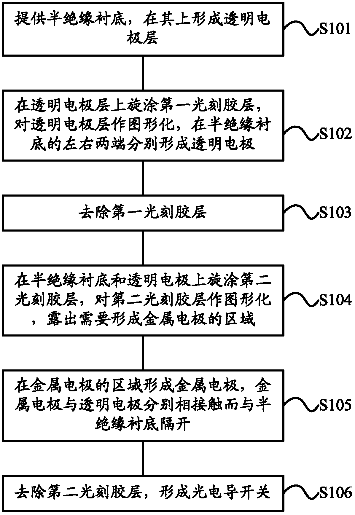
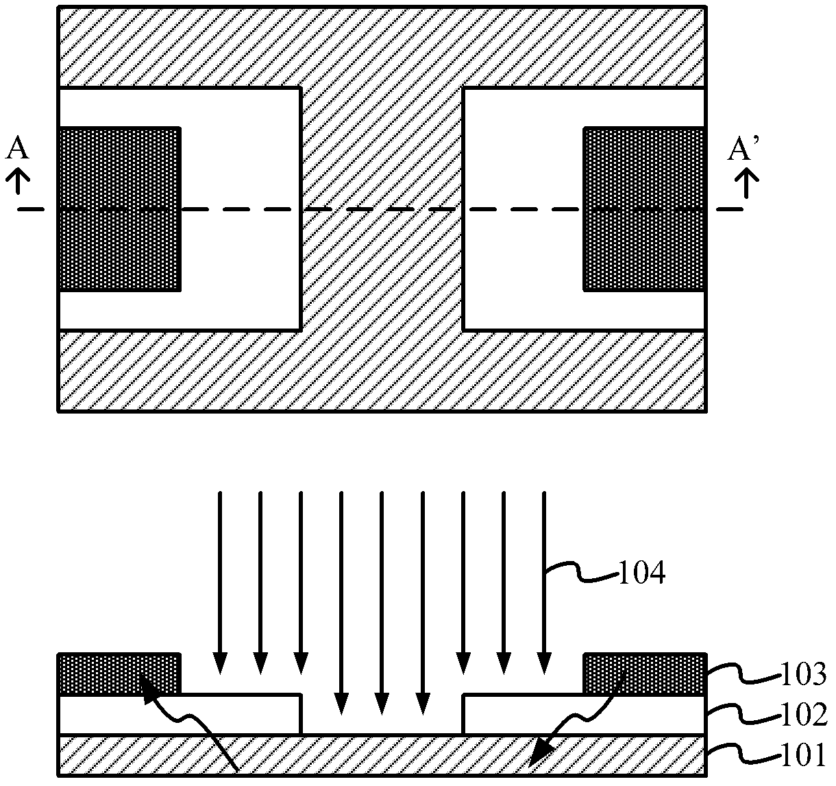
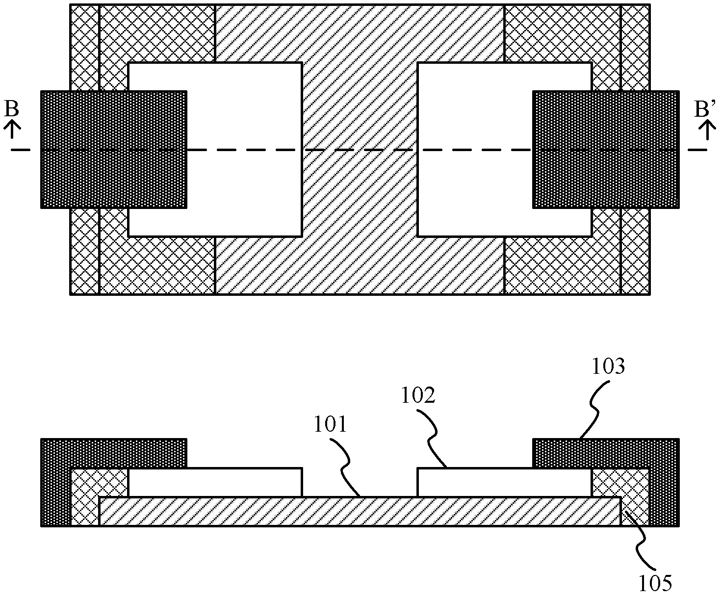
[0064] figure 1 It is a flowchart of a method for manufacturing a photoconductive switch with high withstand voltage and low on-resistance according to an embodiment of the present invention. As shown in the figure, the manufacturing method of the photoconductive switch may include:

[0065] Executing step S101, providing a semi-insulating substrate on which a transpar...


PUM

PropertyMeasurementUnit
Resistivityaaaaaaaaaa
Thicknessaaaaaaaaaa
Wavelengthaaaaaaaaaa

Abstract

The invention provides a method for manufacturing a photoconductive switch high in withstand voltage and low in on resistance, comprising the steps of: providing a semi-insulating substrate, and forming a transparent electrode layer on the semi-insulating substrate; applying a photoresist layer on the transparent electrode layer through spin coating, patterning the transparent electrode layer and forming transparent electrodes at the left and right two ends of the semi-insulating substrate, respectively; applying second photoresist layers on the semi-insulating substrate and the transparent electrode through spin coating, patterning the second photoresist layer and exposing the region for forming a metal electrode; forming the metal electrode which is in contact with the transparent electrodes, respectively, and isolated from the semi-insulating substrate; and removing the second photoresist layers. Accordingly, the invention also provides a photoconductive switch high in withstand voltage and low in on resistance. The method provided by the invention is capable of improving the current density capacity of the switch and reducing the field intensity concentration while guaranteeing a certain electrode spacing, so that the photoconductive switch has low on resistance and high withstand voltage property at the same time.

Description

technical field [0001] The invention relates to the technical field of preparation of high-power semiconductor switching devices, in particular, the invention relates to a photoconductive switch with high withstand voltage and low on-resistance and a manufacturing method thereof. Background technique [0002] Switches are one of the essential components in power electronic circuits, and the properties of switches are particularly important in high-power systems. The so-called high-power system must withstand large voltage and current at the same time. The most direct problem that a large voltage brings to the device is the avalanche breakdown caused by the acceleration of the carrier by the strong electric field, and the thermal breakdown is easy to occur due to the thermal effect under the high current. These two failure modes are difficult problems faced by high-power switching devices. The high-power switch currently used in practical applications is a spark gap switch,...

Claims


Application Information

Patent Timeline
IPC IPC(8): H01L31/18H01L31/08H01L31/0224H01L31/0216
CPCY02P70/50
Inventor 黄维常少辉刘学超王乐星庄击勇陈辉施尔畏
Owner SHANGHAI INST OF CERAMIC CHEM & TECH CHINESE ACAD OF SCI
Why Eureka
Try Eureka