High density interconnect (HDI) plate with mechanic back drilling structure and manufacturing method thereof

A manufacturing method and back-drilling technology, applied in multilayer circuit manufacturing, printed circuit manufacturing, printed circuit components, etc., can solve the problems of complex manufacturing process, high manufacturing cost, and low production efficiency, and achieve simple manufacturing process, The effect of low cost and high production efficiency

Active Publication Date: 2013-04-03
SHENZHEN SUNTAK MULTILAYER PCB
View PDF5 Cites 25 Cited by
  • Summary
  • Abstract
  • Description
  • Claims
  • Application Information

AI Technical Summary

Problems solved by technology

[0009] For this reason, the object of the present invention is to provide a HDI board with a mechanical back-drilling structure and a manufacturing method thereof, so as to solve the problem of multiple pres...

Method used


Image

  • High density interconnect (HDI) plate with mechanic back drilling structure and manufacturing method thereof
  • High density interconnect (HDI) plate with mechanic back drilling structure and manufacturing method thereof

Examples


Embodiment Construction

[0036] In order to illustrate the idea and purpose of the present invention, the present invention will be further described below in conjunction with the accompanying drawings and specific embodiments.

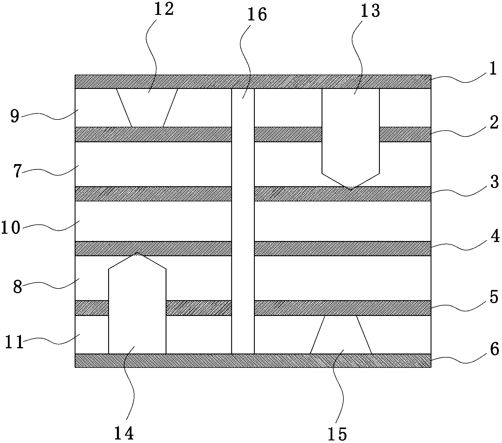
[0037] See figure 1 as shown, figure 1 It is a cross-sectional view of an HDI board with a mechanical back-drilled structure of the present invention. The present invention provides a HDI board with a mechanical back-drilling structure, comprising a first core board 7 and a second core board 8, the first core board 7 is provided with a second copper foil layer 2 on the upper side, and the lower side is provided with The third copper foil layer 3; the upper side of the second core board 8 is provided with the fourth copper foil layer 4, and the fifth copper foil layer 5 is provided below, the third copper foil layer 3 and the fourth copper foil layer 4 The first prepreg 9 is pasted on the second copper foil layer 2, the first prepreg 9 is covered with the first copper foil l...


PUM


Abstract

The invention further provides a high density interconnect (HDI) plate with a mechanic back drilling structure and a manufacturing method thereof. The method comprises that: S1: a first copper foil layer, a first core plate, a second core plate and a sixth copper foil layer are correspondingly subjected to laminating together; S2: the first copper foil layer is subjected to mechanic back drilling processing with the drilling depth reaching a third copper foil layer, and the first copper foil layer, the second copper foil layer and the third copper foil layer are correspondingly connected; S3: the sixth copper foil layer is subjected to the mechanic back drilling processing with the drilling depth reaching a fourth copper foil layer, and the sixth copper foil layer, a fifth copper foil layer and the fourth copper foil layer are correspondingly connected. By adopting a manufacturing way that two core plates are firstly subjected to the laminating one time and then are subjected to the mechanic back drilling processing one time, the production cycle of the HDI plate is greatly shortened, the production cost is reduced, at the same time, the problem of panel expansion caused by multiple times of laminating, laser drillings and abrasive belt grindings is avoided, and the counterpoint accuracy between layers is guaranteed. Compared with the prior art, the HDI plate has the advantages of simple manufacturing process, high production efficiency, low cost and the like.

Description

Technical field: [0001] The invention belongs to the technical field of printed circuit board production, and in particular relates to an HDI board with a mechanical back-drilling structure and a production method thereof. Background technique: [0002] HDI circuit board, also known as high-density interconnection board, is a circuit board with relatively high circuit distribution density using micro-blind buried hole technology, which can reduce the production cost of multi-layer PCB boards, increase circuit density, high reliability, and power Good performance and other advantages. [0003] At present, HDI circuit boards mainly use laser drilling, and its production process is: first lamination → first blind hole window making → first laser drilling → first hole filling electroplating → first abrasive belt grinding Board → the first inner layer pattern → the second pressing → the second blind hole window making → the second laser drilling → the second hole filling electro...

Claims


Application Information

Patent Timeline
IPC IPC(8): H05K1/02H05K3/00H05K3/46
Inventor 黄海蛟姜雪飞李学明叶应才朱拓
Owner SHENZHEN SUNTAK MULTILAYER PCB
Why Eureka
Try Eureka