Optimized light-emitting diode (LED) chip patterned substrate and LED chip

A patterned substrate, LED chip technology, applied in the direction of electrical components, circuits, semiconductor devices, etc., can solve the problems of GaN growth quality damage, lack of design indicators for regular hexagonal pyramid pattern substrate patterns, etc., to improve external quantum efficiency, improve The effect of internal quantum efficiency and excellent light extraction efficiency

Inactive Publication Date: 2013-04-10
SOUTH CHINA UNIV OF TECH
View PDF4 Cites 2 Cited by
  • Summary
  • Abstract
  • Description
  • Claims
  • Application Information

AI Technical Summary

Problems solved by technology

[0004] Even though patterned substrates have greatly improved the light extraction efficiency of LEDs, there are still few studies on regular hexagonal pyramid patterns. For the patterned substrates with regular hexagonal pyramids as the basic pattern, there is still no research result that can clearly point out the optimal pattern inclination angle. , side length, pattern density and other parameters

Method used


Image

  • Optimized light-emitting diode (LED) chip patterned substrate and LED chip
  • Optimized light-emitting diode (LED) chip patterned substrate and LED chip
  • Optimized light-emitting diode (LED) chip patterned substrate and LED chip

Examples


Embodiment 1

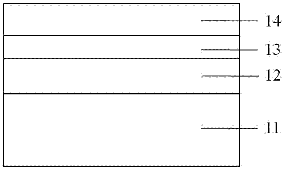
[0024] figure 1 Be the schematic diagram of the LED chip of this embodiment, as figure 1 As shown, it consists of a patterned sapphire substrate 11, an N-type GaN layer 12, an MQW quantum well layer 13, and a P-type GaN layer 14 arranged in sequence.

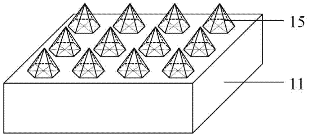
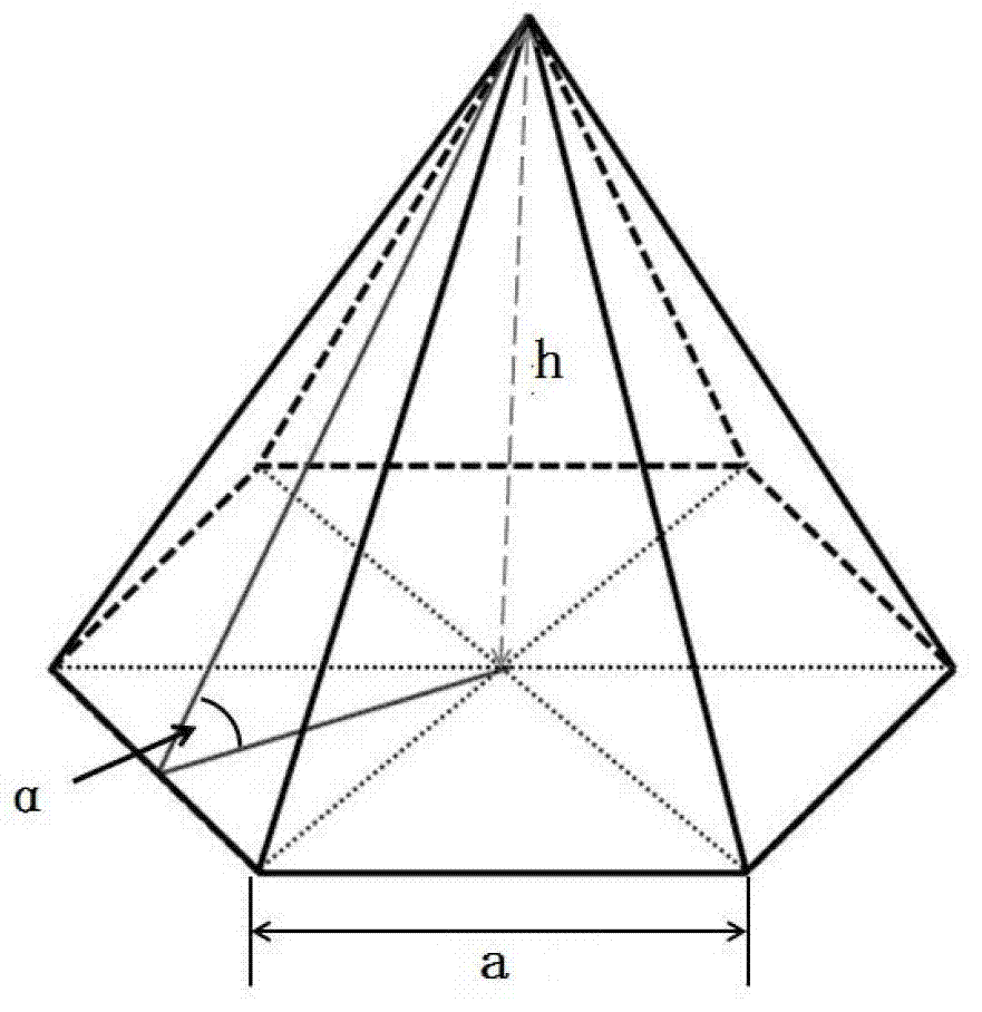
[0025] Such as Figure 2~4 As shown, in the patterned substrate of the LED chip of this embodiment, the pattern of the substrate is composed of a plurality of regular hexagonal pyramids 15 of the same shape arranged on the surface of the substrate, and the inclination angle α of each regular hexagonal pyramid is 60°; The side distance d of the pyramid is 1.0 μ m, and the side distance of adjacent regular hexagonal pyramids is defined as the distance of the bottom surface apex of the adjacent pyramid; the side length a of the regular hexagonal pyramid in the present embodiment is 1.6 μ m; use as Figure 4 The rectangular arrangement shown.

Embodiment 2

[0027] In the patterned substrate of the LED chip of this embodiment, the pattern of the substrate is composed of a plurality of regular hexagonal pyramids of the same shape arranged on the surface of the substrate, and the inclination angle α of each hexagonal pyramid is 55°; The side length a is 2 μm; the side distance d between adjacent regular hexagonal pyramids is 1.2 μm; the plurality of regular hexagonal pyramids with the same shape are arranged in a hexagonal manner.


PUM


Abstract

The invention discloses an optimized light-emitting diode (LED) chip patterned substrate. A Pattern of the LED chip patterned substrate is composed of a plurality of regular hexagonal pyramids with the same shape, the regular hexagonal pyramids are arranged on the surface of the LED chip patterned substrate, dip angles Alpha of the regular hexagonal pyramids are 55 degrees to 60 degrees, and edge distances between regular hexagonal pyramids next to each other are 1.0-1.2 Mum. Compared with the prior art, the LED chip patterned substrate has the advantages that luminous efficiency of the patterned substrate LED chip is greater than that of a ordinary patterned substrate LED chip, available effective light rays are increased greatly, and external quantum efficiency of the LED chip is improved. What is more, the pattern of regular hexagonal pyramids is coincident with a lattice structure of GaN, so the LED chip patterned substrate is beneficial for epitaxial growth of high quality GaN crystals, quality of epitaxy is further improved, and accordingly internal quantum efficiency of the LED chip is improved.

Description

technical field [0001] The invention relates to an LED chip, in particular to an optimized LED patterned substrate and an LED chip. Background technique [0002] The light extraction efficiency of LED depends on internal quantum efficiency and external quantum efficiency. On the one hand, due to the large difference in the lattice constant and thermal expansion coefficient of GaN and sapphire substrates, the crystals of GaN thin films have a density of 10 9 -10 12 cm -2 traversing dislocations, which adversely affect the internal quantum efficiency of GaN-based LEDs. However, with the continuous optimization of GaN epitaxial growth technology, the epitaxial quality of GaN has improved, and the internal quantum efficiency of LEDs has reached more than 90%. On the other hand, GaN has a higher refractive index (n=2.45), and the critical angle [θ c = sin -1 (n air / n GaN )] is only 24.6°, resulting in serious total reflection between the LED chip and the air, and it is ...

Claims


Application Information

Patent Timeline
IPC IPC(8): H01L33/10
Inventor 李国强王海燕何攀贵乔田周仕忠林志霆
Owner SOUTH CHINA UNIV OF TECH
Why Eureka
Try Eureka