Manufacturing method of insulated gate bipolar transistor (IGBT)

A technology of bipolar transistors and manufacturing methods, applied in semiconductor/solid-state device manufacturing, electrical components, circuits, etc., can solve problems such as complex processes, achieve the effect of suppressing diffusion efficiency and improving turn-off rate

Active Publication Date: 2013-04-24
SHANGHAI HUAHONG GRACE SEMICON MFG CORP
View PDF3 Cites 6 Cited by
  • Summary
  • Abstract
  • Description
  • Claims
  • Application Information

AI Technical Summary

Problems solved by technology

But the process is complicated

Method used


Image

  • Manufacturing method of insulated gate bipolar transistor (IGBT)
  • Manufacturing method of insulated gate bipolar transistor (IGBT)
  • Manufacturing method of insulated gate bipolar transistor (IGBT)

Examples


Embodiment Construction

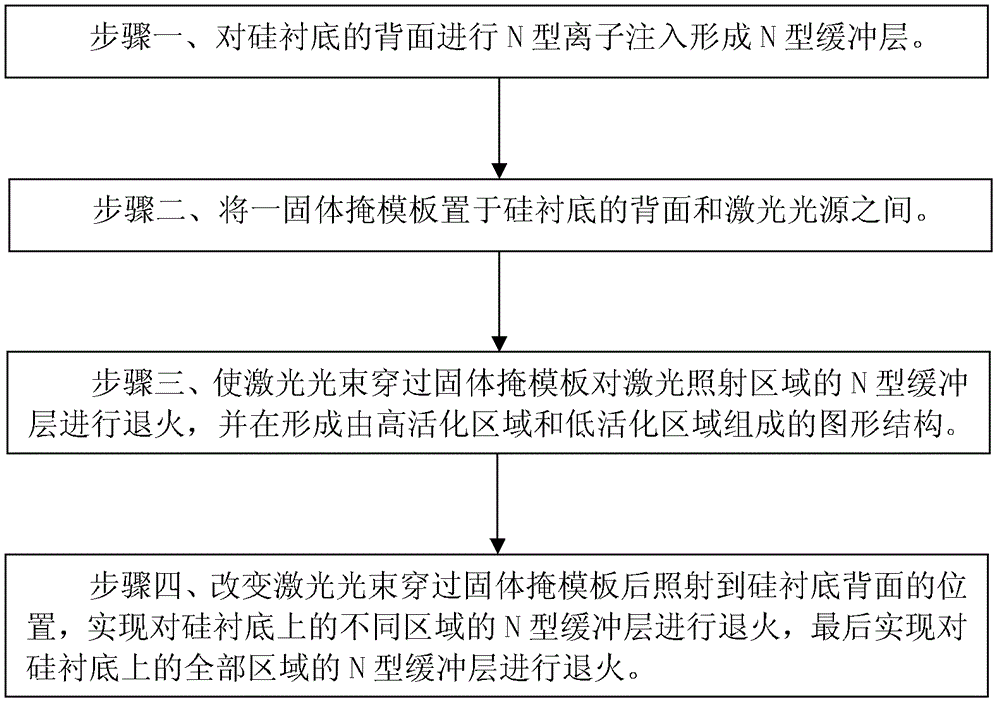
[0032] Such as image 3 Shown is a flow chart of the manufacturing method of the IGBT of the embodiment of the present invention. The manufacturing method of the IGBT of the embodiment of the present invention comprises the following steps:

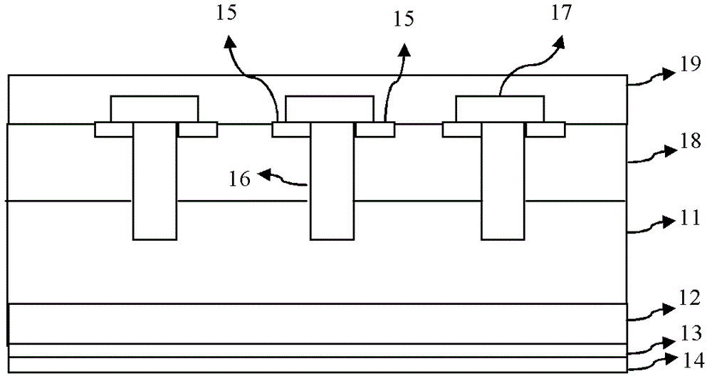
[0033] Such as Figure 4 As shown, the front side process of the insulated gate bipolar transistor is first carried out on the silicon substrate.

[0034] The front process includes the following steps:

[0035] An N-type drift region 11 is formed on the silicon substrate.

[0036] A P-type base region 18 is formed on the N-type drift region 11 .

[0037] A deep trench is formed on the silicon substrate, and polysilicon is filled in the deep trench to form a gate 16 . The gate 16 passes through the P-type base region 18 and enters into the N-type drift region 11 .

[0038] N-type ion implantation is performed in the P-type base region 18 on both sides of the gate 16 to form an N+ doped emitter region 15 . The gate 16 covers the P-t...


PUM


Abstract

The invention discloses a manufacturing method of an insulated gate bipolar transistor (IGBT). A backside technology comprises the following steps that N-iron implantation is performed on a back side of a silicon substrate so as to form an N-buffer; a solid mask plate is placed between the back side of the silicon substrate and a laser light source; a laser beam passes through the solid mask plate and carries out annealing on the N-buffer in a laser irradiation area so as to form a graphic structure which is formed by a high activation area and a low activation area; the laser beam reaches a position of the back side of the silicon substrate after passing through the solid mask plate and the position is changed so as to realize carrying out annealing on the N-buffers of different areas on the silicon substrate; finally, the annealing can be performed on the N-buffers of all the areas on the silicon substrate. By using the method of the invention, a space between the high activation area and the low activation area of the N-buffer can be accurately controlled; when a device is started, stable carrier distribution balance can be formed; when the device is started, diffuser efficiency of a collector region hole can be inhibited and a turn-off rate of the device is increased.

Description

technical field [0001] The invention relates to a method for manufacturing a semiconductor integrated circuit, in particular to a method for manufacturing an insulated gate bipolar transistor. Background technique [0002] Insulated Gate Bipolar Transistor (IGBT) is a voltage-controlled MOS / bipolar composite device, which has the main advantages of both bipolar junction power transistors and power MOSFETs: high input impedance, input Small driving power, small on-resistance, large current capacity, fast switching speed, etc. [0003] Such as figure 1 As shown, the structure diagram of the existing first IGBT includes: [0004] The collector region 13 is composed of a P-type layer formed at the bottom of the silicon substrate, and the collector region electrode 14 is drawn out from the back of the silicon substrate. [0005] The N-type buffer layer (N-buffer) 12 is composed of an N-type ion implantation region implanted from the back of the silicon substrate, and the N-typ...

Claims


Application Information

Patent Timeline
Patent Type & Authority Applications(China)
IPC IPC(8): H01L21/331H01L21/268
Inventor 程晓华彭虎肖胜安
Owner SHANGHAI HUAHONG GRACE SEMICON MFG CORP
Why Eureka
Try Eureka