Formation method for semiconductor device

A semiconductor and device technology, applied in the field of semiconductor device formation, can solve problems such as increased cost, achieve the effects of reduced resistance, reduced process steps, and stable performance

Active Publication Date: 2013-05-01
SHANGHAI HUAHONG GRACE SEMICON MFG CORP
View PDF4 Cites 5 Cited by
  • Summary
  • Abstract
  • Description
  • Claims
  • Application Information

AI Technical Summary

Problems solved by technology

However, adding this layer of mask will increase the corresponding cost. The present invention provid

Method used


Image

  • Formation method for semiconductor device
  • Formation method for semiconductor device
  • Formation method for semiconductor device

Examples


Example Embodiment

[0024] As described in the background art, the existing process for forming resistors in logic circuits or flash memory circuits is still relatively complicated, which is not conducive to reducing process costs.

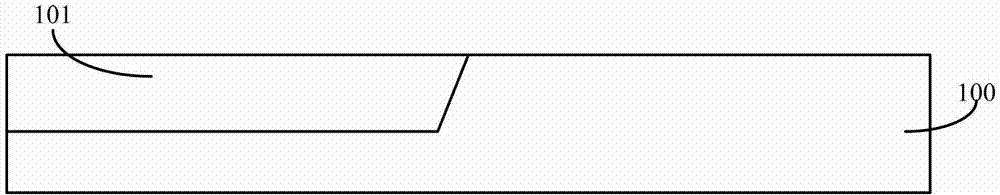
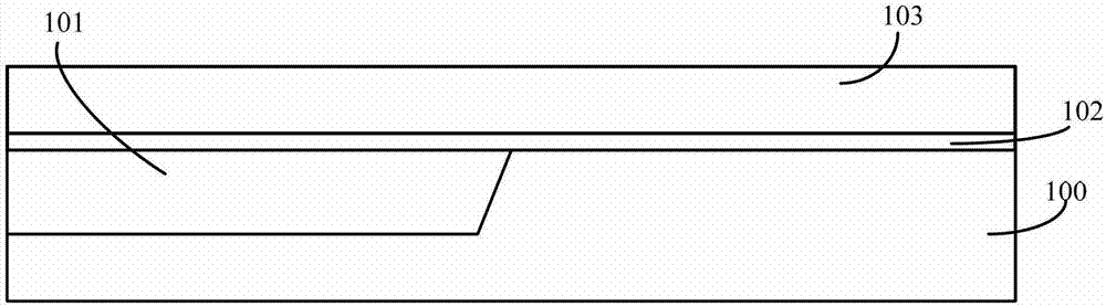
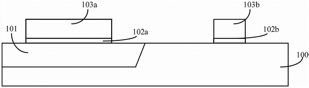
[0025] The inventor of the present invention has discovered through research, please continue to refer to Figure 1 to Figure 3 Since the polysilicon film 103 on the surface of the semiconductor substrate 100 is subsequently used to form the gate electrode layer of the logic transistor, it is necessary to form a metal silicide layer on the surface of the polysilicon film 103 corresponding to the position where the gate electrode layer needs to be formed later, and the metal The silicide layer is used as the electrode of the gate electrode layer of the logic transistor to electrically connect other devices in the circuit or to apply a working voltage.

[0026] However, in order to prevent the formation of a metal silicide layer on the surface of the polysilicon film 103 at ...


PUM


Abstract

The invention discloses a formation method for a semiconductor device. The formation method for the semiconductor device comprises the following steps of: providing a semiconductor substrate, wherein the semiconductor substrate is provided with a storage area, a logic area and a resistance area, and the surface of the semiconductor substrate of the storage area is provided with a flash memory gate structure; forming a first dielectric layer on the surface of the flash memory gate structure and the surface of the resistance area and forming a first polycrystalline silicon layer on the surface of the first dielectric layer; forming second dielectric layers respectively on the surface and the side wall of the first polycrystalline silicon layer of the resistance area and the surface of the semiconductor substrate of the logic area and forming second polycrystalline silicon layers respectively on the second dielectric layers; forming metal silicide layers respectively on the surfaces of the second polycrystalline silicon layers and the surface of the semiconductor substrate of the storage area, the logic area and the resistance area; and forming conductive plugs penetrating the metal silicide layers, the second polycrystalline silicon layers and the second dielectric layers respectively on surfaces of both ends of the first polycrystalline silicon layer of the resistance area. According to the formation method for the semiconductor device, disclosed by the invention, a process step of forming a polyresistor in a flash memory storage circuit can be simplified, and the process time and cost are saved.

Description

technical field [0001] The invention relates to the technical field of semiconductor manufacturing, in particular to a method for forming a semiconductor device. Background technique [0002] Polysilicon resistors are commonly used devices in logic circuits or flash memory circuits. In the design of logic circuits or flash memory circuits, polysilicon layers doped with n-type or p-type ions are often used as resistors, and by adjusting the doped The concentration of impurity ions is used to adjust the resistance value of the polysilicon resistor. [0003] In the prior art, in order to simplify the process steps, polysilicon resistors formed in logic circuits or flash memory circuits are usually formed at the same time as the gate dielectric layer and gate electrode layer of logic transistors, such as figure 1 to Fig. x. [0004] Please refer to figure 1 , providing a semiconductor substrate 100 , the semiconductor substrate 100 has a shallow trench isolation structure 101...

Claims


Application Information

Patent Timeline
IPC IPC(8): H01L21/8247H01L21/02
Inventor 王哲献江红李冰寒高超胡勇于涛
Owner SHANGHAI HUAHONG GRACE SEMICON MFG CORP
Why Eureka
Try Eureka