Light-emitting element
A technology of light-emitting elements and light-emitting layers, applied in the field of organic EL elements), can solve the problems of only observing fluorescence but not phosphorescence, etc., and achieve the effect of high quantum efficiency and long life.
- Summary
- Abstract
- Description
- Claims
- Application Information
AI Technical Summary
Problems solved by technology
Method used
Image

Examples
Embodiment approach 1
[0088] This embodiment mode describes a light-emitting element according to one embodiment of the present invention.
[0089] The light-emitting element of this embodiment includes a light-emitting layer having a guest material as a light-emitting substance, a first organic compound, and a second organic compound. Specifically, a phosphorescent compound is used as a guest material. In addition, in this specification, among the first organic compound and the second organic compound, a material contained in a large amount in the light-emitting layer is referred to as a host material.
[0090] By employing a structure in which the guest material is dispersed in the host material, crystallization of the light-emitting layer can be suppressed. In addition, by suppressing concentration quenching due to a high concentration of the guest material, the luminous efficiency of the light-emitting element can be improved.
[0091] In addition, in the present embodiment, each triplet exci...
Embodiment approach 2
[0180] In this embodiment refer to Figure 16A to Figure 16C A light-emitting element of one embodiment of the present invention will be described.
[0181] Figure 16A It is a diagram showing a light emitting element having an EL layer 102 between a first electrode 103 and a second electrode 108 . Figure 16A The light-emitting element includes: a hole injection layer 701, a hole transport layer 702, a light-emitting layer 703, an electron transport layer 704, an electron injection layer 705 stacked in sequence on a first electrode 103, and a second layer disposed thereon. electrode 108 .
[0182] The first electrode 103 is preferably formed using any metal, alloy, conductive compound, mixture thereof, or the like that has a high work function (more specifically, 4.0 eV or higher). Specifically, for example, indium oxide-tin oxide (ITO: Indium Tin Oxide, indium tin oxide), indium oxide-tin oxide containing silicon or silicon oxide, indium oxide-zinc oxide (Indium Zinc Oxid...
Embodiment 1
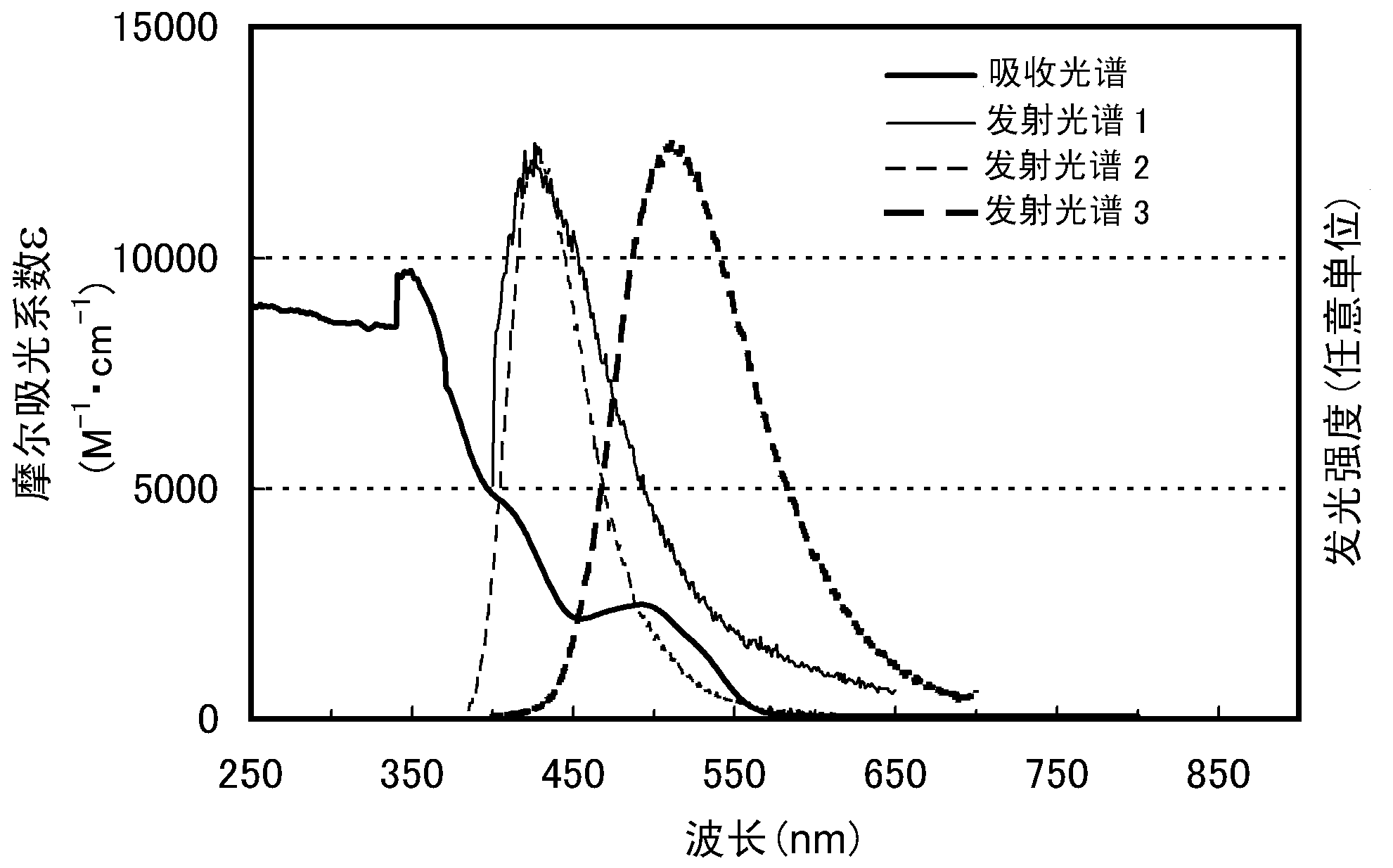
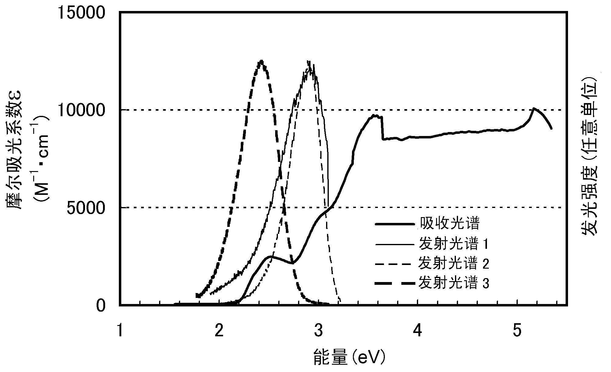
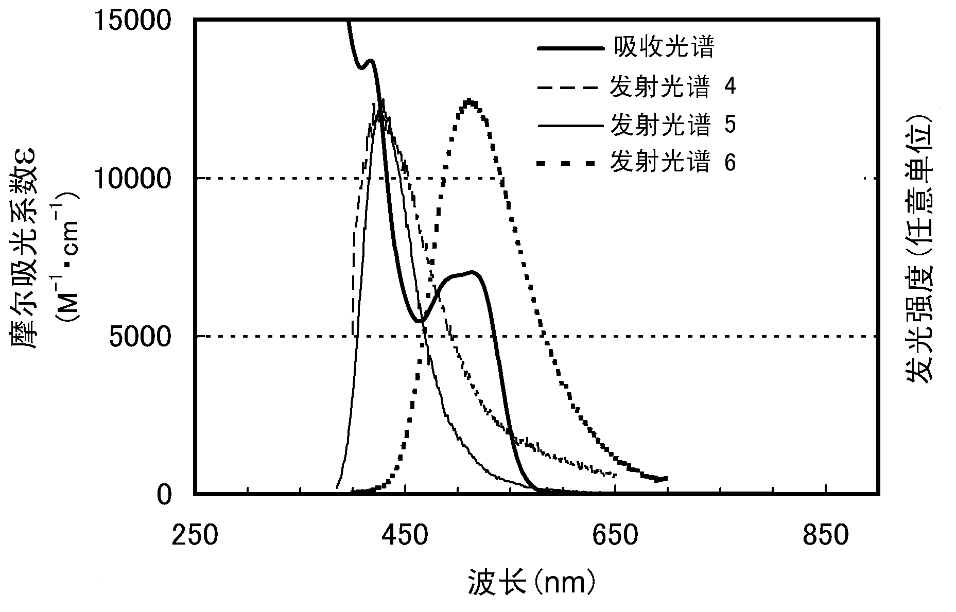
[0242] In this example, refer to Figure 1A and Figure 1B An example of a combination of the first organic compound, the second organic compound, and the phosphorescent compound that can be applied to the light-emitting device of one embodiment of the present invention will be described.
[0243] The phosphorescent compound used in this example is bis(3,5-dimethyl-2-phenylpyrazinium)(dipivaloylmethane)iridium(III) (abbreviation: [Ir(mppr-Me) 2 (dpm)]). The first organic compound used in this example was 2-[3-(dibenzothiophen-4-yl)phenyl]dibenzo[f,h]quinoxaline (abbreviation: 2mDBTPDBq-II). The second organic compound used in this example is 4,4'-bis(1-naphthyl)-4''-(9-phenyl-9H-carbazol-3-yl)triphenylamine (abbreviation: PCBNBB ). Chemical formulas of materials used in this example are shown below.
[0244]
[0245]
[0246] Figure 1A and Figure 1B [Ir(mppr-Me) as a phosphorescent compound is shown 2 (dpm)] of the ultraviolet-visible absorption spectrum (hereinaf...
PUM
 Abstract
Description
Claims
Application Information
 - R&D
- Intellectual Property
- Life Sciences
- Materials
- Tech Scout
- Unparalleled Data Quality
- Higher Quality Content
- 60% Fewer Hallucinations
Browse by: Latest US Patents, China's latest patents, Technical Efficacy Thesaurus, Application Domain, Technology Topic, Popular Technical Reports.
© 2025 PatSnap. All rights reserved.Legal|Privacy policy|Modern Slavery Act Transparency Statement|Sitemap|About US| Contact US: help@patsnap.com