Interconnect Fabrication Method

A manufacturing method and interconnection structure technology, which are applied in semiconductor/solid-state device manufacturing, electrical components, circuits, etc., can solve problems such as damage to the outline of the low-k dielectric layer 100, reduction in the quality of metal wiring, and short-circuiting of devices. Reliability and electrical performance, avoiding copper filling voids, effect of good copper filling performance

Active Publication Date: 2015-11-25
SEMICON MFG INT (SHANGHAI) CORP
View PDF4 Cites 0 Cited by
  • Summary
  • Abstract
  • Description
  • Claims
  • Application Information

AI Technical Summary

Problems solved by technology

[0004] In order to allow the device to obtain good integration and reliability, the sidewall of the metal wiring trench 104 must be straight or nearly straight, however, as figure 1 As shown, due to the weak mechanical properties of the low-k dielectric, when the low-k dielectric layer 100 is formed by a plasma dry etching process, the plasma will cause damage 101 to the low-k dielectric layer on the sidewall of the metal wiring trench; In order to improve the electromigration resistance, adhesion and other surface characteristics of the copper filling of the metal wiring, generally before copper electroplating is performed on the metal wiring trench 102, a Ta / TaN physical vapor deposition process is applied on the metal wiring. The outer surface of the wiring trench 102 forms a barrier layer and a barrier seed layer (barrierseed layer) 103, and the Ta / TaN high-energy attack effect will damage the outline of the low-k dielectric layer 100 at the bottom of the metal wiring trench 102 (as shown by 104 in the figure Shown), reduce the quality of metal wiring, may cause short circuit, open circuit and parasitic capacitance of the device, affecting the reliability and electrical performance of the device

Method used


Image

  • Interconnect Fabrication Method
  • Interconnect Fabrication Method
  • Interconnect Fabrication Method

Examples


Embodiment Construction

[0029] The method for manufacturing the interconnection structure proposed by the present invention will be further described in detail below with reference to the accompanying drawings and specific embodiments.

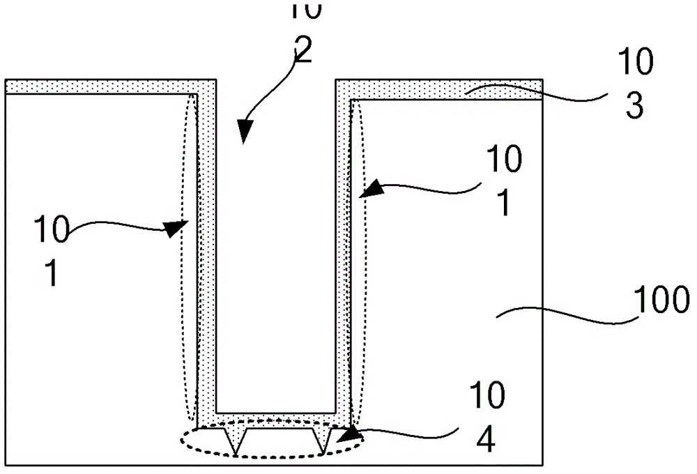
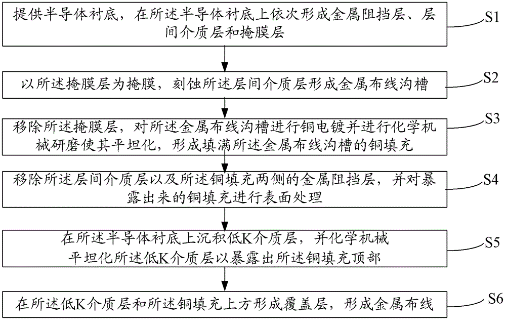
[0030] like figure 2 As shown, the present invention proposes a method for manufacturing an interconnection structure, comprising the following steps:

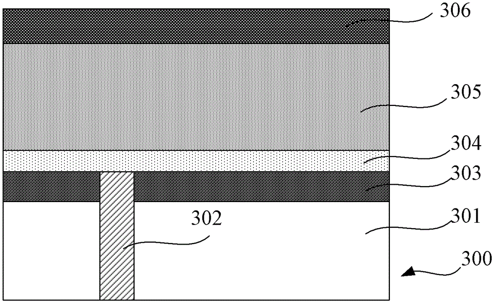
[0031] S1, providing a semiconductor substrate, and sequentially forming a metal barrier layer, an interlayer dielectric layer, and a mask layer on the semiconductor substrate;

[0032] S2, using the mask layer as a mask, etching the interlayer dielectric layer to form metal wiring trenches;

[0033] S3, removing the mask layer, performing copper electroplating on the metal wiring groove and performing chemical mechanical polishing to make it planarized, forming a copper filling that fills the metal wiring groove;

[0034] S4, removing the interlayer dielectric layer and the metal barrier layers on both sides of t...


PUM


Abstract

The invention provides a manufacturing method of an interconnection structure. First, a metal wiring groove is etched in an inter-lamination dielectric layer; and then, a k dielectric layer is deposited after copper electroplating on the metal wiring groove is finished and the inter-lamination dielectric layer is removed. The conditions that low k mediums on two sides are damaged in the process of etching the metal wiring groove in a metal wiring technology in the prior art, and that low k mediums on the bottom of the metal wiring groove are damaged after Ta / TaN and other inner blocking layers and seed layers are used are avoided. Further more, a metal blocking layer plays a role in an electrode when copper electroplating is conducted on the metal wiring groove to ensure that the copper vertically and upwards grows along the bottom of the through hole. The metal blocking layer can prevent the copper from filling gaps, and therefore good copper filling performance is obtained, and metal wiring quality and reliability and electrical properties of a device are improved.

Description

technical field [0001] The invention relates to the field of semiconductor manufacturing, in particular to a method for manufacturing an interconnection structure. Background technique [0002] In the integrated circuit manufacturing process of 90nm and below nodes, the Cu-CMP damascene process (damascenes process) is usually used to manufacture metal wiring, generally forming a single damascene structure and a double damascene structure, and the single damascene structure usually only uses a single layer of metal wiring The manufacturing method is changed from the traditional "metal etching + dielectric layer filling" to "dielectric layer etching + metal filling". The dual damascene structure is usually combined through via holes and metal wiring, and only the metal filling step is required. The manufacturing process can be simplified, and it is mostly used in the manufacture of multilayer interconnection structures. [0003] In the prior art, in order to meet the requirem...

Claims


Application Information

Patent Timeline
Patent Type & Authority Patents(China)
IPC IPC(8): H01L21/768
Inventor 王冬江张海洋
Owner SEMICON MFG INT (SHANGHAI) CORP
Why Eureka
Try Eureka