
Quantum well terahertz detector

A terahertz detector and quantum well technology, applied in the field of terahertz detectors, can solve the problems of inability to contribute to the photocurrent of the external circuit of the detector, inability to respond to THz radiation, etc., and achieve the suppression of dark current and phonon scattering probability, The effect of reducing dark current and improving detection rate

Inactive Publication Date: 2013-05-15
CHANGZHOU INST OF OPTOELECTRONICS TECH +1
View PDF3 Cites 4 Cited by
  • Summary
  • Abstract
  • Description
  • Claims
  • Application Information

AI Technical Summary

Problems solved by technology

However, the purpose of using electron transitions between hydrogen-like donor levels for THz detection in quantum well THz detectors has not yet been realized.
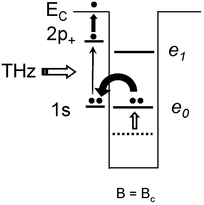
This is because the donor impurity electrons in the potential well layer of the quantum well structure are still bound at the bottom of the potential well even if they undergo a transition from the ground state to the highly excited state after absorbing THz radiation. , cannot contribute to the photocurrent in the circuit outside the detector; for the donor impurity electrons in the barrier layer of the quantum well structure, because the position of the donor energy level in the ground state is lower than the position of the subband energy level in the potential well Much higher, resulting in no electron occupation on the ground-state donor energy level, and thus no response to incident THz radiation

Method used


Image

  • Quantum well terahertz detector
  • Quantum well terahertz detector
  • Quantum well terahertz detector

Examples


Embodiment 1

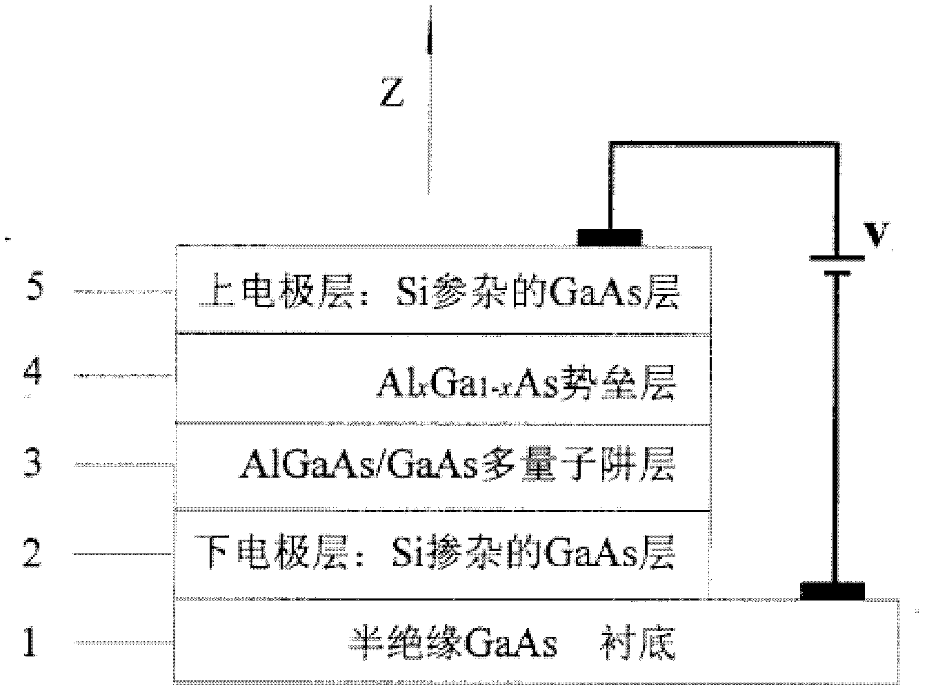
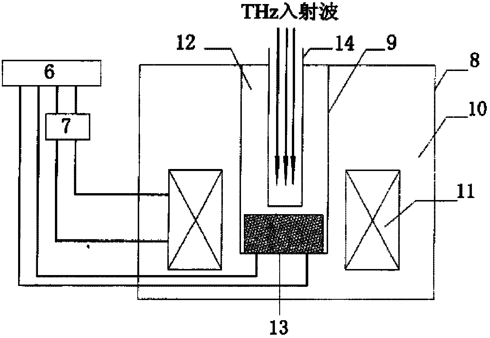
[0021] See figure 1 with figure 2 , a quantum well terahertz detector in this embodiment includes a multi-quantum well semiconductor chip 13 and a superconducting magnet system.

[0022] See figure 1 , the multi-quantum well chip 13 of this embodiment utilizes typical semiconductor material epitaxial growth technology, such as molecular beam epitaxy technology, metal-organic chemical vapor deposition technology, etc., and the preparation process is mature. Sequential growth on a semi-insulating GaAs substrate 1:

[0023] Si-doped GaAs lower electrode layer 2 with a thickness of 800 nm;

[0024] Alternately growing 30 or 50 cycles of multiple quantum well layers 3 composed of AlGaAs barrier layers and GaAs potential well layers;

[0025] 20nm thick AlGaAs barrier layer 4;

[0026] Si-doped GaAs upper electrode layer 5 with a thickness of 400 nm.

[0027] The height of the AlxGa1-xAs barrier layer in the multi-quantum well layer 3 is adjusted by the Al composition x, and ...


PUM


Abstract

The invention discloses a quantum well terahertz detector which is composed of a multiple quantum well chip and a superconducting magnet system. Interaction between a donor level in a barrier layer in the multiple quantum well chip and a sub-band energy level in a potential well layer is regulated effectively by exerting an applied magnetic field so that electrons are transferred from a ground state sub-band energy level in the potential well layer to the donor level in the barrier layer, and incidence THz radiation is detected by utilizing electron transition between the donor levels in the barrier layer. According to the quantum well terahertz detector, after the applied magnetic field increases to a critical magnetic field Bc, due to the fact that THz detecting can be conducted by utilizing electron transition between the donor levels, the quantum well terahertz detector is free from grating coupling or angle lapping coupling of 45 degrees, the THz radiation is absorbed and responded under the condition of normal incidence, the defects caused by principle of an existing quantum well structure detector are overcome, and responsivity can be improved substantially.

Description

technical field [0001] The invention relates to a terahertz (THz) detector with a semiconductor multi-quantum well structure. Background technique [0002] THz electromagnetic radiation with a wavelength between microwave and infrared light in the range of 30 microns to 1000 microns has important applications in many fields such as wireless communication, public safety, astronomy, medical imaging and ultrafast spectroscopy. Among them, the semiconductor quantum well THz detector is one of the technical approaches to realize ideal high-efficiency solid-state THz detection, and is a research hotspot in the THz field. This detector is based on the multi-quantum well structure infrared detector (QWIP), by reducing the barrier height in the barrier layer to reduce the energy level spacing of the subbands in the potential well layer, the detection range is developed to cover the THz band. Adjusting the structure of this quantum well THz detector with a controllable growth method...

Claims


Application Information

Patent Timeline
IPC IPC(8): H01L31/101H01L31/0248G01J1/42
Inventor 张波余晨辉陆卫李宁陈平平甄红楼王文娟李志锋李天信陈效双
Owner CHANGZHOU INST OF OPTOELECTRONICS TECH
Learn More