


Quick Research
Generate reliable direction feasibility study reports for your R&D in just a few steps.

Technical Q&A
Discover and master advanced knowledge NOW. Basics, ideas, possibilities, all at once.

Find Solutions
As an expert in R&D theories, this can generate solutions to your technical problems instantly.

Evaluate Feasibility
Analyze your overall solution with one click, know your potential R&D risks in advance.

Monitor Landscape
Get weekly tech updates, stay abreast of the latest tech innovations and key insights.
Spin injection electrode production method
A technology of spin injection and manufacturing method, which is applied in the manufacturing/processing of electromagnetic devices, manufacturing of inductors/transformers/magnets, circuits, etc., and can solve the problems that spin injection electrodes have not been reported
- Summary
- Abstract
- Description
- Claims
- Application Information
AI Technical Summary
Problems solved by technology
Method used
Image

Examples
Embodiment )
[0068] Hereinafter, the present invention will be described in more detail through examples.
Embodiment 1)
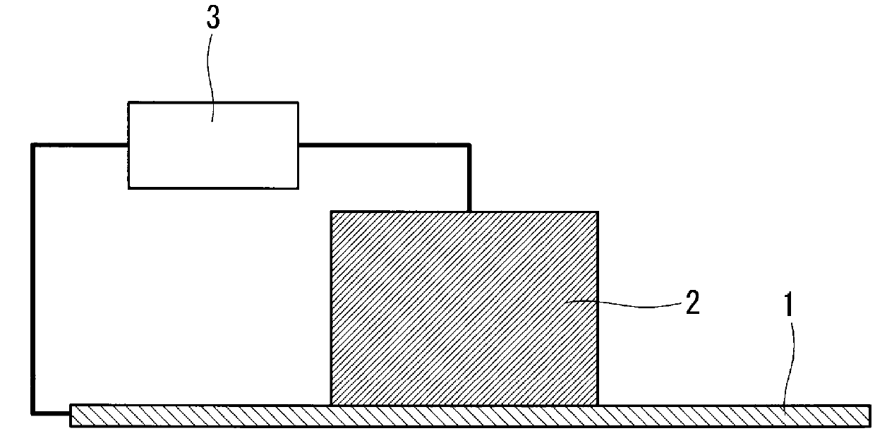
[0070] First, graphene 1 was prepared referring to the description in Science, vol.306, p.666-p.669 (2004). Specifically, the cellophane tape was pressed against 1 mm thick highly oriented pyrolytic graphite (Highly Oriented Pyrolytic Graphite: HOPG) and the wafer was peeled off, and the cellophane tape was pressed again on the peeled wafer and a part of it was peeled off to produce a thinner sheet. The operation of partially peeling off the obtained sheet with a cellophane tape was repeated several times, and then the HOPG sheet on the cellophane tape was rubbed against a sapphire substrate. When evaluated using an atomic force microscope (AFM), the thickness of the graphene 1 on the sapphire substrate was about 1±0.5 nm. This corresponds to the thickness of several layers of graphene. It has been confirmed by another method that the same result can be obtained even if the substrate is made of a material other than sapphire, as long as it has the strength to arrange the flak...
Embodiment 2)
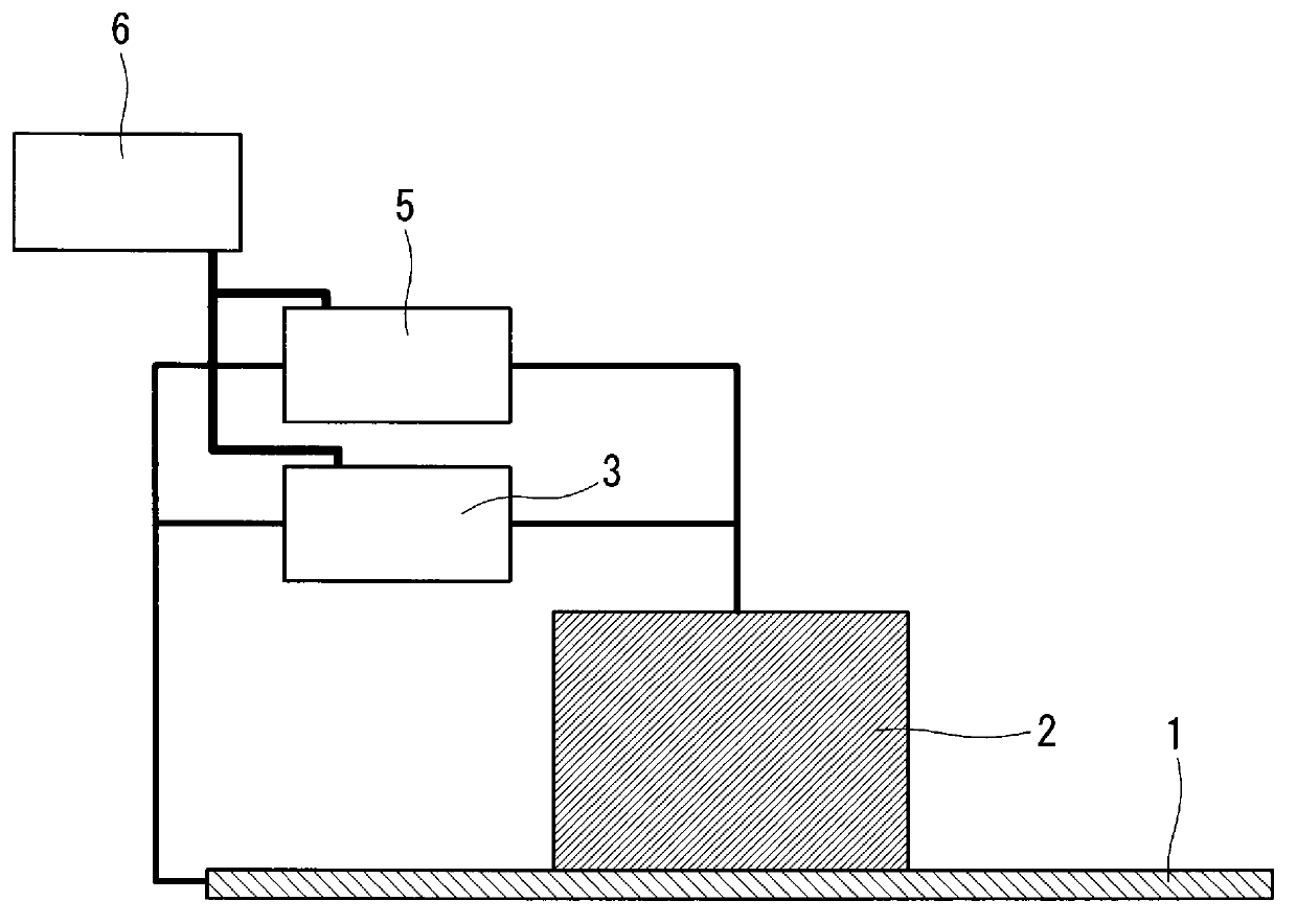
[0083] In Example 2, the change of the interface resistance value in the case of changing the applied electrical bias (resistance change ratio R / R 0 )did an evaluation. In the same manner as in Example 1, a laminate of sapphire substrate 7 , graphene 1 , and iron oxide 2 to which an electrical bias was applied was produced.
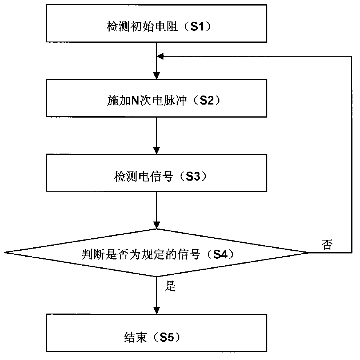
[0084] When the magnitude of the applied pulse voltage is increased from 3.5V, Figure 8 Shown as the resistance change ratio R / R 0 The number of times Np of pulse application that changes rapidly decreases. On the other hand, this Np increases when the magnitude of the applied pulse voltage is made smaller from 3.5V.
[0085] This Np increases when the magnitude of the applied pulse voltage is fixed at 3.5 V and the pulse width is shortened from 1 μs, and decreases when it becomes longer. Thus, it was confirmed that the interface resistance value between graphene 1 / iron oxide 2 can be controlled and set by controlling the application conditions of th...
PUM
| Property | Measurement | Unit |
|---|---|---|
| lattice constant | aaaaa | aaaaa |
| lattice constant | aaaaa | aaaaa |
| wavelength | aaaaa | aaaaa |
Abstract
Description
Claims
Application Information
 - R&D Engineer
- R&D Manager
- IP Professional
- Industry Leading Data Capabilities
- Powerful AI technology
- Patent DNA Extraction
Browse by: Latest US Patents, China's latest patents, Technical Efficacy Thesaurus, Application Domain, Technology Topic, Popular Technical Reports.
© 2024 PatSnap. All rights reserved.Legal|Privacy policy|Modern Slavery Act Transparency Statement|Sitemap|About US| Contact US: help@patsnap.com