Parasitic crosswise PNP triode and manufacturing method thereof in germanium-silicon heterojunction bipolar transistor (HBT) technology

A PNP triode, lateral technology, used in semiconductor/solid-state device manufacturing, electrical components, circuits, etc., can solve the problems of high cost, complex deep trench isolation process, high epitaxy cost, improve frequency characteristics, reduce connection resistance, The effect of reducing the area

Active Publication Date: 2013-06-05
SHANGHAI HUAHONG GRACE SEMICON MFG CORP
View PDF2 Cites 0 Cited by
  • Summary
  • Abstract
  • Description
  • Claims
  • Application Information

AI Technical Summary

Problems solved by technology

The parasitic lateral PNP device technology in the existing SiGe HBT is mature and reliable, but the main disadvantages are: epitaxial gr

Method used


Image

  • Parasitic crosswise PNP triode and manufacturing method thereof in germanium-silicon heterojunction bipolar transistor (HBT) technology
  • Parasitic crosswise PNP triode and manufacturing method thereof in germanium-silicon heterojunction bipolar transistor (HBT) technology
  • Parasitic crosswise PNP triode and manufacturing method thereof in germanium-silicon heterojunction bipolar transistor (HBT) technology

Examples


Example Embodiment

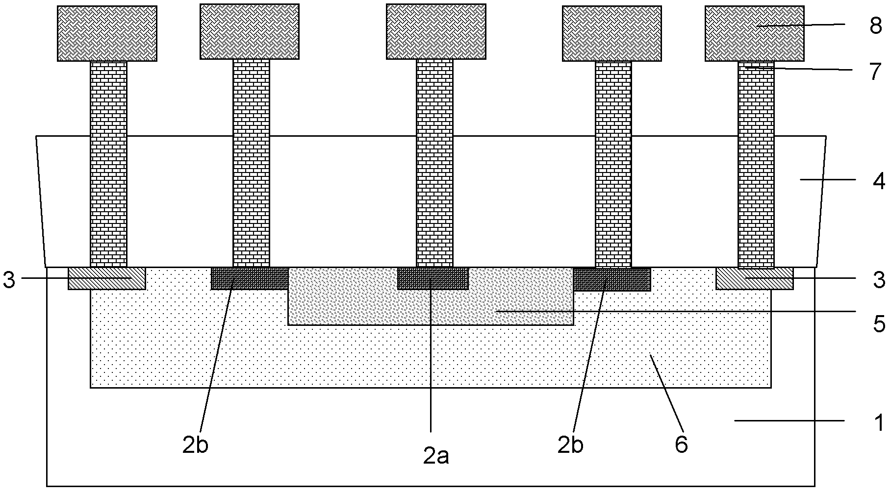
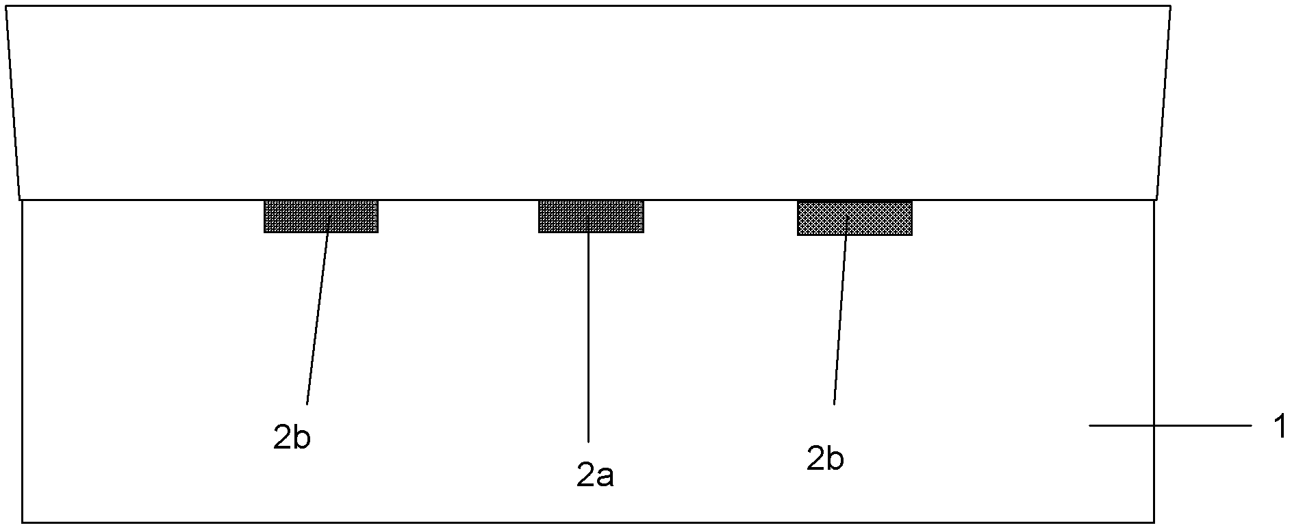
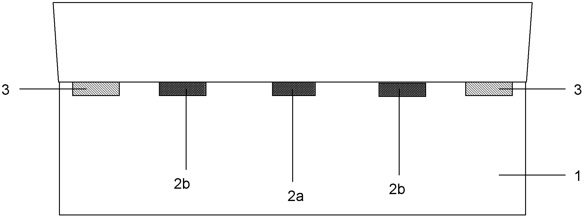
[0022] like figure 1 Shown is the device structure diagram of the embodiment of the present invention. The parasitic lateral PNP transistor in the silicon germanium HBT process of the embodiment of the present invention is formed on the P-type silicon substrate 1, and the active region is isolated by the shallow trench field oxygen 4, that is, the isolation structure of the active region is shallow trench isolation (STI), include:

[0023] The base region is composed of an N well 5 formed in the silicon substrate 1 at the bottom of the shallow trench field oxygen 4 .

[0024] The emitter region is composed of the first P-type pseudo-buried layer 2a formed in the N well 5; a deep hole contact 7 is formed in the shallow trench field oxygen 4 on the top of the first P-type pseudo-buried layer 2a And leads to the emitter.

[0025] The collector region is composed of a second P-type pseudo-buried layer 2b formed at the bottom of the shallow trench field oxygen 4 and located on t...


PUM


Abstract

The invention discloses a parasitic crosswise PNP triode in a germanium-silicon heterojunction bipolar transistor (HBT) technology. A base region comprises a N trap which is formed at the bottom of shallow groove field oxygen, an emission region comprises a first P-type fake buried layer which is formed in the N trap, and a collector region comprises second P-type fake buried layers which are formed at the bottom of the shallow groove field oxygen and are arranged on the side face of the N trap. The N-type deep trap is arranged at the bottom of the shallow groove field oxygen, and the base region, the emission region and the collector region are all encircled by the N-type deep trap. N-type fake buried layers are connected with the base region through the N-type deep trap. An emitter, a collector and a base are all elicited in a contact mode through a deep hole formed in the top of each N-type fake buried layer. The invention further discloses a manufacturing method of the parasitic crosswise PNP triode in the germanium-silicon HBT technology. The parasitic crosswise PNP triode and the manufacturing method of the parasitic crosswise PNP triode in the germanium-silicon HBT technology can effectively reduce area of a device, is incapable of occupying the area of an active region, can reduce connecting resistance between the collector and a base end, and can remarkably improve frequency characteristics of the device under the condition that a current gain factor of the device is not influenced.

Description

technical field [0001] The invention relates to the field of semiconductor integrated circuit manufacturing, in particular to a parasitic lateral PNP transistor in a silicon-germanium HBT process; the invention also relates to a method for manufacturing the parasitic lateral PNP transistor in a silicon-germanium HBT process. Background technique [0002] In radio frequency applications, higher and higher device characteristic frequencies are required. Although RFCMOS can achieve higher frequencies in advanced process technologies, it is still difficult to fully meet radio frequency requirements. For example, it is difficult to achieve characteristic frequencies above 40GHz, and advanced technology The research and development cost of compound semiconductors is also very high; compound semiconductors can realize very high characteristic frequency devices, but due to the disadvantages of high material cost and small size, and the toxicity of most compound semiconductors, its ap...

Claims


Application Information

Patent Timeline
IPC IPC(8): H01L29/737H01L29/36H01L21/331
Inventor 陈帆陈雄斌薛恺周克然潘嘉李昊蔡莹陈曦
Owner SHANGHAI HUAHONG GRACE SEMICON MFG CORP
Why Eureka
Try Eureka