Supercharge Your Innovation With Domain-Expert AI Agents!

Ceramic base copper clad laminate and production method thereof

A technology of ceramic copper clad laminates and ceramic substrates, which is applied in circuit substrate materials, multilayer circuit manufacturing, printed circuit components, etc., can solve the problem that adhesion is difficult to guarantee, the sputtered copper plating layer is not dense enough, and the peeling resistance is not enough. requirements and other issues to achieve the effect of reducing product costs and improving market competitiveness

Active Publication Date: 2013-06-05
SHENZHEN GAGIET CERAMIC CIRCUIT TECH
View PDF4 Cites 24 Cited by
  • Summary
  • Abstract
  • Description
  • Claims
  • Application Information

AI Technical Summary

Problems solved by technology

In the prior art, the following processes are mostly used on ceramic substrates: cleaning - vacuum sputtering - electroless copper deposition - circuit wiring - dry film application, exposure, development - electroplating copper thickening - chemical etching, etc. In the prior art, in the vacuum sputtering process, a layer of titanium is first sputtered and then a layer of copper is sputtered. However, in practical applications, because titanium metal is particularly easy to passivate, sputtering The copper plating layer is not dense enough, and it is difficult to ensure that the titanium layer will not be oxidized and passivated during subsequent processing.
Therefore, the adhesion between the thickened copper plating layer and the titanium layer is difficult to guarantee, and it is easy to cause the anti-peeling strength to fail to meet the requirements

Method used


Image

  • Ceramic base copper clad laminate and production method thereof
  • Ceramic base copper clad laminate and production method thereof
  • Ceramic base copper clad laminate and production method thereof

Examples


Embodiment Construction

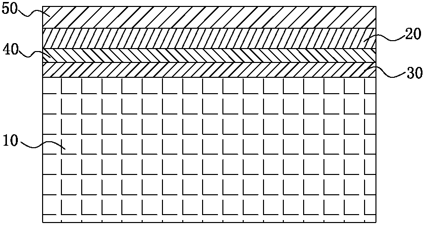
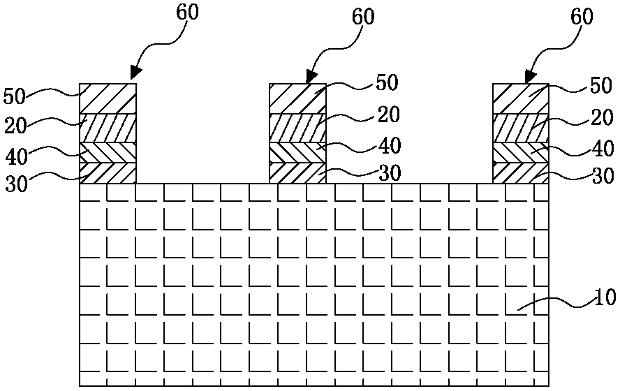
[0026] Please refer to figure 2 As shown, it shows the specific structure of a preferred embodiment of the present invention: a ceramic copper clad laminate, including a ceramic substrate 10, on which a titanium layer 20, a nickel layer 30 and a copper layer 40 are sequentially arranged, The titanium layer 20 is attached to the ceramic substrate 10, the nickel layer 30 is attached to the titanium layer 20, and the copper layer 40 is attached to the nickel layer 30; the thickness of the titanium layer 20 is 30-100 nanometers, and the nickel layer The thickness of 30 is 30-100 nanometers, and the thickness of the copper layer 40 is 50-150 nanometers; a thickened copper layer 50 is electroplated on the copper layer 40 .

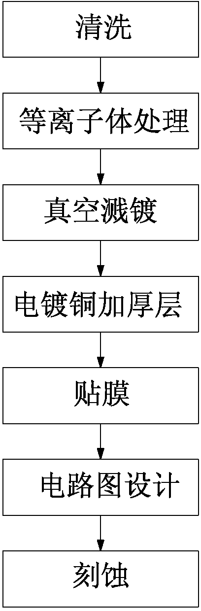
[0027] Such as figure 1 Shown, a kind of preparation method of ceramic copper clad laminate and circuit board thereof comprises the following steps:

[0028] (1) Cleaning: cleaning the ceramic substrate 10 with alcohol, and then baking at 200° C. for 60 minut...


PUM

PropertyMeasurementUnit
thicknessaaaaaaaaaa
thicknessaaaaaaaaaa
thicknessaaaaaaaaaa

Abstract

The invention discloses a ceramic base copper clad laminate and a production method thereof. The ceramic base copper clad laminate comprises a ceramic substrate. A titanium layer, a nickel layer and a copper layer are sequentially arranged on the ceramic substrate. The titanium layer is attached to the ceramic substrate, the nickel layer is attached to the titanium layer, the copper layer is attached to the nickel layer, and a copper thickened layer is further electroplated on the copper layer. The production method of the ceramic base copper clad laminate includes the steps of cleaning, plasma treatments, vacuum splattering, thickened copper plating and the like. A good adhesive force exists between the titanium layer and the ceramic substrate, a good adhesive force exists between the nickel layer and the titanium layer, and a good adhesive force exists between the nickel layer and the copper layer. Therefore, the copper layer can be connected with the ceramic substrate firmly so as to facilitate follow-up treatments. For the ceramic base copper clad laminate, different circuits can be designed by customers according to different circuit requirements, and only with one additional etching process can a ceramic printed circuit board (PCB) be obtained. The ceramic base copper clad laminate meets the requirements of customers for PCBs with different circuit designs, facilitates mass production, and lowers production cost.

Description

technical field [0001] The invention relates to the technical field of circuit boards and preparation methods thereof, in particular to an aluminum oxide or aluminum nitride ceramic copper-clad board and a preparation method thereof. Background technique [0002] Ceramic materials have the characteristics of high thermal conductivity, low dielectric constant, thermal expansion coefficient similar to chips, high heat resistance and electrical insulation. Ceramic materials have been widely used in electronic products and electronic equipment. In the prior art, the following processes are mostly used on ceramic substrates: cleaning - vacuum sputtering - electroless copper deposition - circuit wiring - dry film application, exposure, development - electroplating copper thickening - chemical etching, etc. In the prior art, in the vacuum sputtering process, a layer of titanium is first sputtered and then a layer of copper is sputtered. However, in practical applications, because t...

Claims


Application Information

Patent Timeline
Patent Type & Authority Applications(China)
IPC IPC(8): H05K1/03H05K3/46
Inventor 翟克峰
Owner SHENZHEN GAGIET CERAMIC CIRCUIT TECH
Features
  • R&D
  • Intellectual Property
  • Life Sciences
  • Materials
  • Tech Scout
  • Unparalleled Data Quality
  • Higher Quality Content
  • 60% Fewer Hallucinations
Learn More