Silicon-based thin film material with sandwich structure and preparation method and application thereof

A silicon-based film and sandwich technology, applied in metal material coating process, ion implantation plating, coating, etc., can solve the problems of limited improvement of single-layer film and material cycle performance can not meet the needs, etc., to achieve improved repeatability The effects of stability, increased thickness, and simple preparation process

Active Publication Date: 2013-06-12
NANKAI UNIV
View PDF4 Cites 11 Cited by
  • Summary
  • Abstract
  • Description
  • Claims
  • Application Information

AI Technical Summary

Problems solved by technology

In recent years, thin-film materials have developed rapidly, and silicon thin-film has high specific capacity and good cycle performance. Therefore, silicon thin-film electrode materials have been paid more and more attention by people, such as using magnetron sputtering or chemical deposition to deposit silicon thin films on current collectors; using chemical vapor deposition , depositing nano-silicon films on the surface of graphite, etc. These methods also improve the cycle performance of silicon to a certain extent, but the improvement of single-layer films is limited, and the cycle performance of materials still cannot meet the needs.

Method used


Image

  • Silicon-based thin film material with sandwich structure and preparation method and application thereof
  • Silicon-based thin film material with sandwich structure and preparation method and application thereof
  • Silicon-based thin film material with sandwich structure and preparation method and application thereof

Examples


Embodiment 1

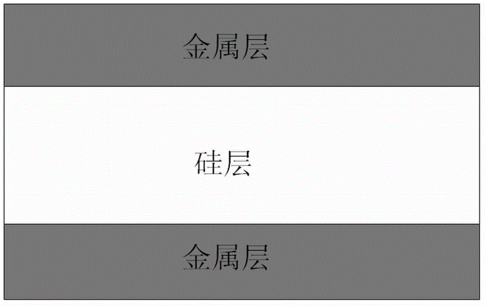
[0032] A silicon-based thin film material with a sandwich structure, such as figure 1 As shown, the laminated sandwich structure is composed of Zn layer, Si layer and Zn layer, the thickness of the Zn layer film is 50nm, and the thickness of the Si layer film is 100nm; the sandwich structure Zn-Si-Zn film material is prepared by alternate sputtering process, Proceed as follows:

[0033] 1) Install the cleaned substrate stainless steel mesh, Zn target and n-type Si target at the sample position in the magnetron sputtering chamber, the purity of the target is greater than 99.9%, the target points to the sample position, and the distance between the target and the substrate is 5cm ;

[0034] 2) Vacuum the cavity background to 1.0×10 -3 Below Pa, feed Ar gas with a purity of more than 99.99% into the cavity, the flow rate is 10sccm, adjust the air pressure in the sputtering chamber to 0.5Pa, the substrate temperature is 25°C, and the substrate rotation speed is 25r / min, and the ...

Embodiment 2

[0041] A silicon-based thin film material with a sandwich structure, such as figure 1 As shown, the laminated sandwich structure is composed of Al layer, Si layer and Al layer, the thickness of the Al layer film is 100nm, and the thickness of the Si layer film is 250nm; the sandwich structure Al-Si-Al film material is prepared by alternate sputtering process, Proceed as follows:

[0042] 1) Install the cleaned substrate foam nickel, Al target and n-type Si target at the sample position in the magnetron sputtering chamber. The purity of the target is greater than 99.9%. The target points to the sample position, and the distance between the target and the substrate is 8cm ;

[0043] 2) Vacuum the cavity background to 1.0×10 -3 Below Pa, feed Ar gas with a purity of more than 99.99% into the chamber, the flow rate is 15sccm, adjust the air pressure in the sputtering chamber to 0.5Pa, the substrate temperature to 200°C, and the substrate speed to 15r / min, turn off the metal Al t...

Embodiment 3

[0050] A silicon-based thin film material with a sandwich structure, such as figure 1 As shown, the laminated sandwich structure is composed of Y layer, Si layer and Y layer, the thickness of the Y layer film is 50nm, and the thickness of the Si layer film is 450nm; the sandwich structure Y-Si-Y film material is prepared by alternate sputtering process, Proceed as follows:

[0051] 1) Install the cleaned substrate foam copper, Y target and p-type Si target at the sample position in the magnetron sputtering chamber. The purity of the target is greater than 99.9%. The target points to the sample position, and the distance between the target and the substrate is 10cm ;

[0052] 2) Vacuum the cavity background to 1.0×10 -3 Below Pa, feed Ar gas with a purity of more than 99.99% into the cavity, the flow rate is 18sccm, adjust the air pressure in the sputtering chamber to 0.5Pa, the substrate temperature to 300°C, and the substrate rotation speed to 20r / min, and close the metal Y...


PUM

PropertyMeasurementUnit
thicknessaaaaaaaaaa
thicknessaaaaaaaaaa
thicknessaaaaaaaaaa

Abstract

The invention relates to a silicon-based thin film material with a sandwich structure. According to the silicon-based thin film material, a laminated sandwich structure consists of a metal layer, a silicon layer and a metal layer, wherein the metal layers have the thickness of 20-100 nm, and the Si layer has the thickness of 60 nm to 9.8 microns. According to a preparation method of the silicon-based thin film material, an alternate sputtering process for metallic targets of the metal layers and a silicon target of the Si layer is adopted, a metallic conductive attached-layer thin film is firstly prepared on a substrate, a Si thin film is then prepared, and a metallic thin layer finally covers the surface of the Si thin film, thereby forming the sandwich structure. The silicon-based thin film material and the preparation method of the silicon-based thin film material have the advantages that the silicon-based thin film material with the sandwich structure is used as a negative pole material of a lithium battery, and then, the larger volume change of the silicon-based thin film material during lithium ion deionizing / embedding is effectively inhibited, so that the lithium battery has higher energy density, cycle stability and multiplying factor performance; and the method is simple in process and lower in cost and is hopefully applied to high-energy and high-power thin-film batteries.

Description

technical field [0001] The invention relates to a silicon-based negative electrode material for a lithium battery and a preparation method thereof, in particular to a silicon-based thin film material with a sandwich structure and a preparation method and application thereof. Background technique [0002] Lithium-ion batteries play an important role in the mobile electronics market due to their high energy and power density. After the expansion of research technology and application fields in recent years, lithium-ion batteries have begun to move towards diversification. They are used in electric vehicles and energy storage power stations. There is also a huge demand in other fields. [0003] The technological breakthrough of cathode materials has laid the foundation for the application of lithium batteries to move from electronic terminal equipment such as mobile phones and notebook computers to electric vehicles and energy storage technology. It is already close to the the...

Claims


Application Information

Patent Timeline
Patent Type & Authority Applications(China)
IPC IPC(8): B32B33/00H01M4/13C23C14/35C23C14/16
CPCY02E60/122Y02E60/10
Inventor 陶占良郭爽李海霞陈军程方益梁静
Owner NANKAI UNIV
Why Eureka
Try Eureka