Chemical method for synthesising silver selenide semiconductor photoelectric film material in situ at room temperature

A photoelectric thin film and in-situ synthesis technology, applied in the field of material chemistry, can solve the problems of complex film formation process, high toxicity of reactants, high production cost, etc., and achieve the effect of simple reaction device, controllable reaction process and convenient operation

Active Publication Date: 2013-06-12
XUCHANG UNIV
View PDF4 Cites 8 Cited by
  • Summary
  • Abstract
  • Description
  • Claims
  • Application Information

AI Technical Summary

Problems solved by technology

[0008] The problem to be solved by the present invention is: to overcome the current preparation of Ag 2 In the preparation process of Se semiconductor thin film materials, there are shortcomings such as dependence on high vacuum, high energy consumption, high production cost, high toxicity of reactants, and complicated film formation process. It provides an in-situ synthesis of silver selenide semiconductor with low or no energy consumption at room temperature. A chemical method for photoelectric thin films, which is simple to operate, low in production cost, and has broad industrial application prospects

Method used


Image

  • Chemical method for synthesising silver selenide semiconductor photoelectric film material in situ at room temperature
  • Chemical method for synthesising silver selenide semiconductor photoelectric film material in situ at room temperature
  • Chemical method for synthesising silver selenide semiconductor photoelectric film material in situ at room temperature

Examples


Embodiment 1

[0038] Ag 2 Preparation of Se Binary Compound Semiconductor Photoelectric Thin Film Materials

[0039] 1. Preparation: Clean the ITO conductive glass with detergent and deionized water for 20 minutes, and then use concentrated ammonia water (25% by mass) / hydrogen peroxide (30% by mass) / deionized water (volume ratio: 1: The mixed solution of 2:5) was treated at 80°C for 30 minutes, and finally ultrasonically cleaned with deionized water for 20 minutes. The treated ITO conductive glass was dried at 80°C and stored in a clean desiccator for later use. Use magnetron sputtering technology to sputter a single silver layer with a thickness of 100nm on the ITO conductive glass substrate, and use film thickness monitoring (FTM) to control the thickness of the silver layer. The obtained ITO conductive glass with a simple silver layer is stored in a desiccator for use .

[0040] 2. Reaction steps: take 0.6gNa 2 S·9H 2 O was dissolved in 30 ml of deionized water, and then 0.01 g of Se...

Embodiment 2

[0043] Ag 2 Preparation of Se Binary Compound Semiconductor Photoelectric Thin Film Materials

[0044] 1. Preparatory work: Same as in Example 1, sputtering a single silver layer with a thickness of 250nm on the ITO conductive glass substrate.

[0045] 2. Reaction steps: weigh 0.6gNa 2 S·9H 2 O was dissolved in 30 ml of deionized water, and then 0.01 g of Se powder was dissolved in the Na 2 In the S aqueous solution, the temperature was kept at 25° C. for 30 min to obtain an orange-yellow solution. Place the ITO conductive glass sputtered with 250nmAg into the above orange solution, react at 25°C for 7min, and take out the sample.

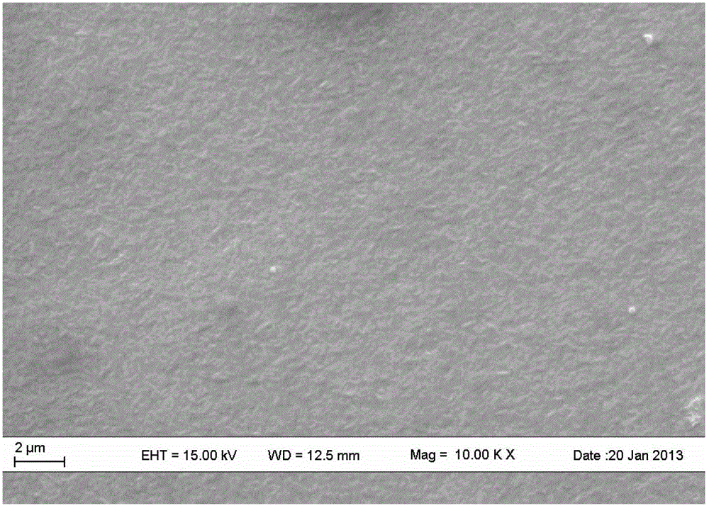
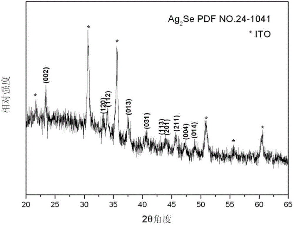
[0046] 3, aftertreatment: with embodiment 1. The product obtained was a silver gray film. diagram 2-1 SEM photographs of the obtained samples, Figure 2-2 It is the XRD figure of the obtained sample, and its PDF card number is: 24-1041, which proves that the obtained product is a pure silver selenide material.

Embodiment 3

[0048] Ag 2 Preparation of Se Binary Compound Semiconductor Photoelectric Thin Film Materials

[0049] 1. Preparatory work: Same as in Example 1, sputtering a single silver layer with a thickness of 250nm on the ITO conductive glass substrate.

[0050] 2. Reaction steps: weigh 0.6gNa 2 S·9H 2 O was dissolved in 30 ml of deionized water, and then 0.01 g of Se powder was dissolved in the Na 2 In S aqueous solution, keep the temperature at 7° C. for 30 min to obtain an orange-yellow solution, and dilute the solution to 125 ml. Place the ITO conductive glass sputtered with 250nmAg into the above orange solution, react at 7°C for 51min, and take out the sample.

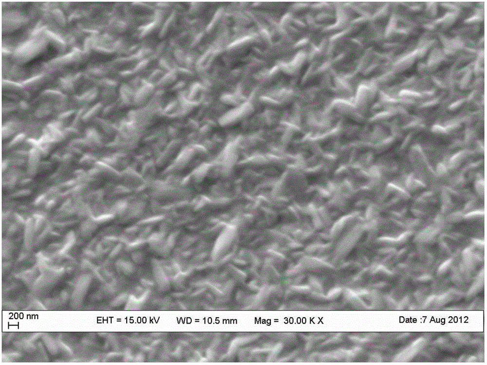
[0051] 3, aftertreatment: with embodiment 1. The product obtained was a silver gray film. Figure 3-1 SEM photographs of the obtained samples, Figure 3-2 It is the XRD figure of the obtained sample, and its PDF card number is: 24-1041, which proves that the obtained product is a pure silver selenide material. The ...


PUM

PropertyMeasurementUnit
phase transition temperatureaaaaaaaaaa
thicknessaaaaaaaaaa
thicknessaaaaaaaaaa

Abstract

The invention provides a chemical method for synthesising a silver selenide semiconductor photoelectric film material in situ at a room temperature. The method comprises the following steps of: dissolving elementary-substance Se powder in Na2S aqueous solution to form orange-yellow solution; placing a substrate material sputtered with an elementary-substance silver film on the surface and the solution aforementioned in the same container; and growing the Ag2Se semiconductor photoelectric film material on the surface of the substrate in situ via a short-time reaction in a temperature range from 7 to 35 DEG C. The reactants are low in price, has no need of being further purified, green and environment-friendly, and any surfactant or other chemical additives are not required; room-temperature reaction conditions are moderate, energy consumption is little, and influence on a conducting substrate is avoided; and the chemical method is fast in reaction, convenient in operation, and controllable in process. The chemical method provided by the invention overcomes the defects of dependence on high vacuum, high energy consumption and high production cost, high reactant toxicity, complex film-forming process and the like of the existing preparation process for an Ag2Se semiconductor photoelectric film material, and is beneficial to large-scale production and industrial application.

Description

technical field [0001] The invention belongs to the technical field of material chemistry, and in particular relates to a chemical method for large-area synthesis of silver selenide semiconductor photoelectric thin film materials at room temperature. Background technique [0002] Group I-VI Binary Compound Ag 2 Se is a high carrier concentration (approximately 10 19 cm -3 ) and high charge mobility (μ n =1990cm 2 / Vs) n-type semiconductor material; this material has a high-temperature stable phase (α phase) and a low-temperature stable phase (β phase), and the phase transition temperature is 135°C, wherein the high-temperature stable phase has the properties of a fast ion conductor and can be used as a solid state Electrolyte, low-temperature stable phase with high Seebeck coefficient, high electrical conductivity and low lattice thermal conductivity, is an ideal thermoelectric material; the material has a wide spectral absorption range, which can extend from the ultravi...

Claims


Application Information

Patent Timeline
Patent Type & Authority Applications(China)
IPC IPC(8): C03C17/22
Inventor 郑直王承相雷岩魏杰范丽波
Owner XUCHANG UNIV
Why Eureka
Try Eureka