U-shaped channel tunneling transistor with laminated structure and preparation method thereof

A technology of tunneling transistors and stacked structures, which is applied in the manufacture of semiconductor/solid-state devices, semiconductor devices, electrical components, etc. The effect of band bending, increasing turn-on current, and reducing tunneling length

Inactive Publication Date: 2013-06-12
FUDAN UNIV
View PDF2 Cites 10 Cited by
  • Summary
  • Abstract
  • Description
  • Claims
  • Application Information

AI Technical Summary

Problems solved by technology

[0004] However, when the tunneling transistor is working, the energy band gap between the source region and the chann

Method used


Image

  • U-shaped channel tunneling transistor with laminated structure and preparation method thereof
  • U-shaped channel tunneling transistor with laminated structure and preparation method thereof
  • U-shaped channel tunneling transistor with laminated structure and preparation method thereof

Examples


Embodiment Construction

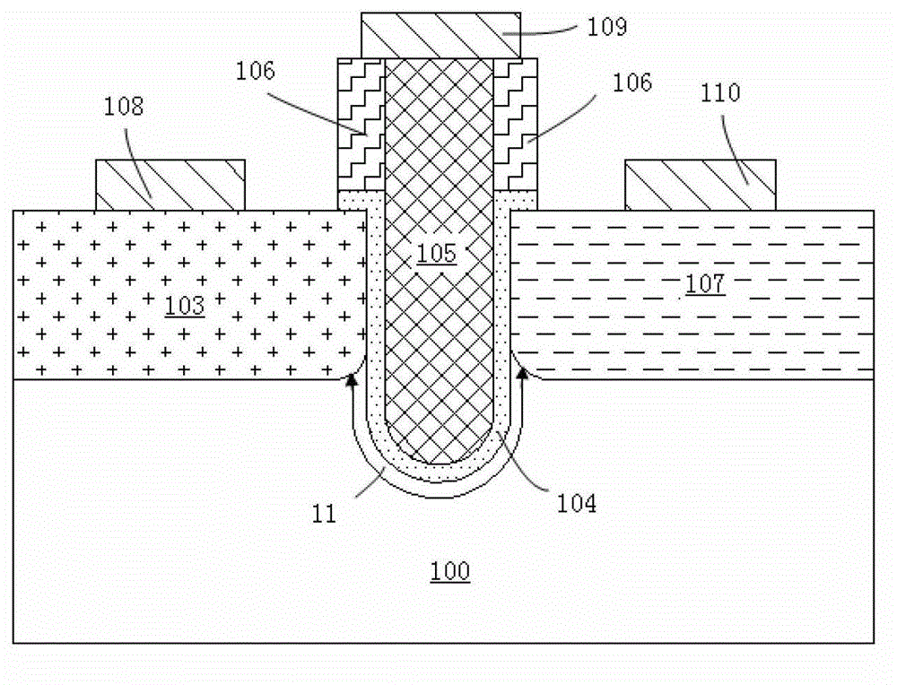
[0033] The present invention will be further described in detail below in conjunction with the accompanying drawings and specific embodiments. In the drawings, for the convenience of illustration, the thicknesses of layers and regions are enlarged or reduced, and the sizes shown do not represent actual sizes. Although these figures do not fully reflect the actual size of the device, they still completely reflect the mutual positions between the regions and the constituent structures, especially the upper-lower and adjacent relationships between the constituent structures.

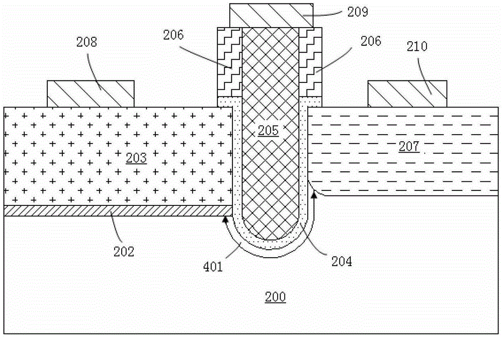
[0034] figure 2 It is an embodiment of the U-shaped channel tunneling transistor with stacked structure disclosed by the present invention, and it is a cross-sectional view along the channel length direction of the device. Such as figure 2 , the semiconductor substrate 200 with the first doping type can be single crystal silicon, polycrystalline silicon or silicon-on-insulator, and is doped with a low co...


PUM

PropertyMeasurementUnit
Physical thicknessaaaaaaaaaa

Abstract

The invention belongs to the technical field of semiconductor devices, and particularly relates to a U-shaped channel tunneling transistor with a laminated structure and a preparation method thereof. According to the invention, a highly doped silicon layer of which the doping type is opposite to that of a SiGe source area is formed under the SiGe source area of the tunneling transistor by an epitaxial growth method; and the forbidden bandwidth of the SiGe is narrower than that of silicon, so that the band bending degree between the source area and a channel region can be improved, then the length of tunneling can be reduced and the tunneling efficiency is improved. The U-shaped channel tunneling transistor with the laminated structure which is provided by the invention can substantially improve firing current and reduces subthreshold swing under the circumstance that shutdown current is not influenced.

Description

technical field [0001] The invention belongs to the technical field of semiconductor devices, and in particular relates to a U-shaped channel tunneling transistor and a manufacturing method thereof. Background technique [0002] With the continuous development of the integrated circuit industry, metal-oxide-semiconductor field-effect transistor (MOSFET) integrated circuit technology driven by proportional reduction has entered the nanometer size, and will continue to follow Moore's law to further reduce the device size to meet Chip miniaturization, high density, high speed and system integration requirements. Today's integrated circuit device technology node is already at about 50 nanometers, and the leakage current between the source and drain of MOSFETs increases rapidly as the channel length shrinks. Especially when the channel length drops below 30nm, it is necessary to use a new type of device to obtain a smaller leakage current, thereby reducing chip power consumption...

Claims


Application Information

Patent Timeline
IPC IPC(8): H01L29/78H01L29/06H01L21/336
Inventor 王玮王鹏飞张卫
Owner FUDAN UNIV
Why Eureka
Try Eureka