Preforming device for semiconductor cavity

A tablet pressing device and semiconductor technology, which is applied in semiconductor/solid-state device manufacturing, discharge tubes, electrical components, etc., can solve the problems affecting production schedule and production cost, affecting production cost, uneven ion implantation dose and depth, etc., and achieve improvement Tabletting quality and tableting efficiency, improved structural stability, easy and fast tablet delivery

Active Publication Date: 2013-06-19
中科九微科技有限公司
View PDF6 Cites 0 Cited by
  • Summary
  • Abstract
  • Description
  • Claims
  • Application Information

AI Technical Summary

Problems solved by technology

The traditional point pressure method mainly has the following problems: 1. The silicon wafer is unevenly stressed, which causes the silicon wafer to break during the process or the contact between the silicon wafer and the carrier table is not solid, causing the bias electric field above the silicon wafer to be uneven. uniform, which in turn leads to uneven ion implantation dose and depth, and the damage to the tablet to be pressed caused by unstable tablet quality directly affects the production cost; 2. The bias electric field is distorted near the pressure point, causing the implanted ions to Focusing makes the edge effect of injection more serious; 3. The point pressure type is not conducive to the automatic loading process, the production efficiency is not high, and it also affects the production schedule and production cost

Method used


Image

  • Preforming device for semiconductor cavity
  • Preforming device for semiconductor cavity
  • Preforming device for semiconductor cavity

Examples


Embodiment Construction

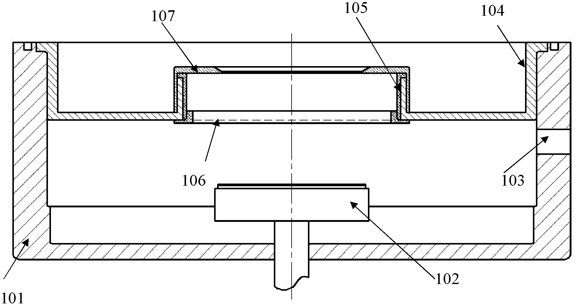
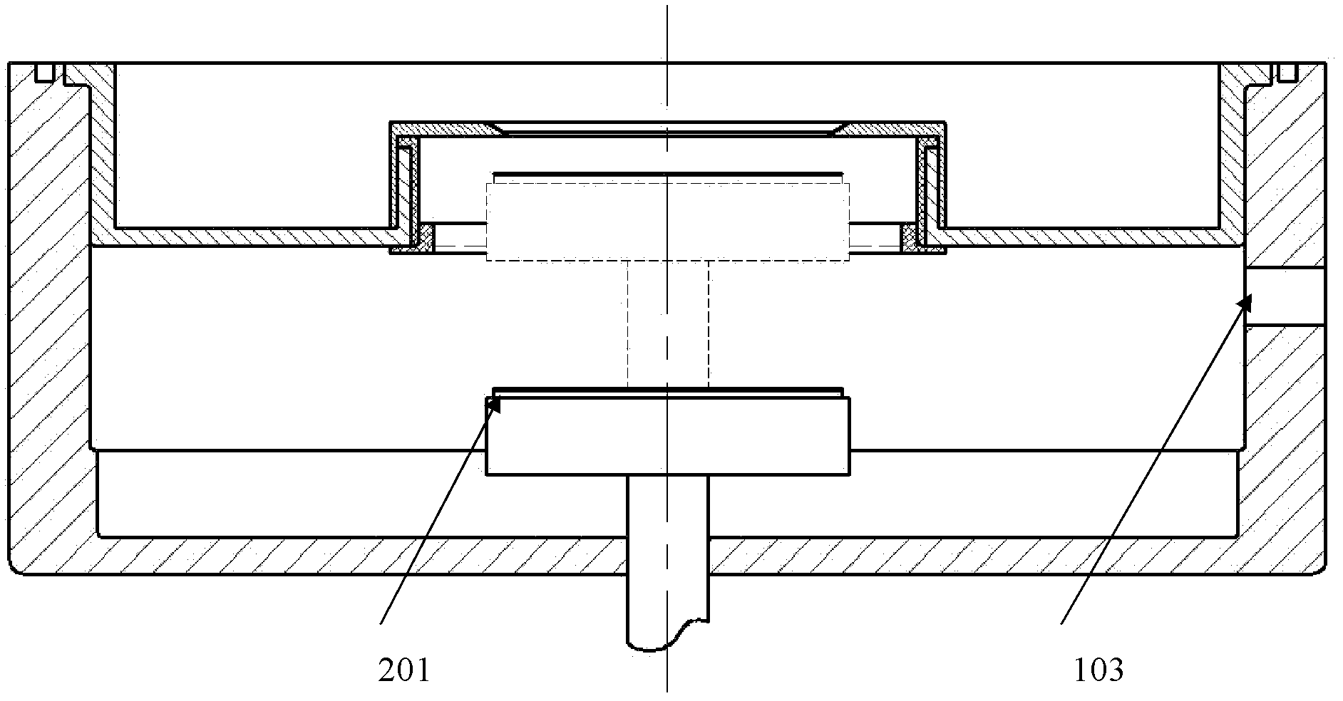
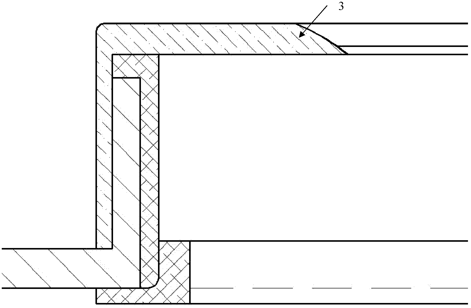
[0023] see figure 1 , A tablet pressing device for a semiconductor chamber provided by an embodiment of the present invention includes a reaction chamber 101 , a chamber lining 104 , a tablet press frame 107 , a polytetrafluoroethylene protective sleeve 105 , a support bracket 106 and a slide loading mechanism 102 . The reaction chamber 101 is provided with a sheet feeding hole 103 . The slide mechanism 102 is an electrostatic chuck or a slide table. Tablet press rack 107 is arranged on the upper half of reaction chamber 101, and the height of tablet press rack is low, makes the space for feeding sheet large, is beneficial to the smooth and rapid progress of the sheet feeding process of the sheet feeding mechanism, and also provides a certain degree of protection for the tablet feeding mechanism. Independent design space. The tablet press frame 107 is in a "concave" shape, and both ends of the tablet press frame 107 have through holes, and the chamber lining 104 is plugged i...


PUM


Abstract

The invention discloses performing device for a semiconductor cavity. The performing device for the semiconductor cavity comprises a reaction cavity, a preforming frame and a chip-mounting mechanism. The preforming frame is arranged at the upper portion of the reaction cavity. A cavity liner is arranged inside the reaction cavity and connected with the preforming device. The chip-mounting mechanism is arranged at the lower end of the preforming frame. The performing device for the semiconductor cavity not only increases chip-sending space, enables chip-sending to be fast, improves stability of structure of the preforming frame, and further improves preforming quality and efficiency.

Description

technical field [0001] The invention relates to the technical field of plasma implantation, in particular to a tablet pressing device for a semiconductor chamber. Background technique [0002] In the semiconductor process, the mainstream impurity doping technology is the beamline ion implantation technology (IonImplantation, II). This method generates plasma from the ion source, extracts the required ion components through mass spectrometry analysis, and then accelerates the ions to a certain energy. Implanted into a semiconductor substrate (such as a silicon wafer). This method requires complex mass spectrometry and scanning devices, low injection efficiency, complex structure, and extremely high cost. [0003] With the further shrinking of the feature size of integrated circuits, the ion implantation energy needs to be further reduced to below 1000 electron volts (sub-KeV). Negative effect. Therefore, a novel plasma immersion implantation technique (Plasma Immersion Ion...

Claims


Application Information

Patent Timeline
Patent Type & Authority Applications(China)
IPC IPC(8): H01J37/32H01L21/67
Inventor 李超波屈芙蓉陈瑶刘传钦夏洋
Owner 中科九微科技有限公司
Why Eureka
Try Eureka