Method for manufacturing brightness-improved GaN-based light emitting diode (LED) chip

A technology of LED chips and manufacturing methods, applied in the direction of electrical components, circuits, semiconductor devices, etc.

Inactive Publication Date: 2013-06-19
INST OF SEMICONDUCTORS - CHINESE ACAD OF SCI
View PDF4 Cites 6 Cited by
  • Summary
  • Abstract
  • Description
  • Claims
  • Application Information

AI Technical Summary

Problems solved by technology

In addition, when making ITO transparent electrodes, ITO is used as the ohmic contact metal layer with P-GaN and N-GaN at the

Method used


Image

  • Method for manufacturing brightness-improved GaN-based light emitting diode (LED) chip
  • Method for manufacturing brightness-improved GaN-based light emitting diode (LED) chip
  • Method for manufacturing brightness-improved GaN-based light emitting diode (LED) chip

Examples


Embodiment Construction

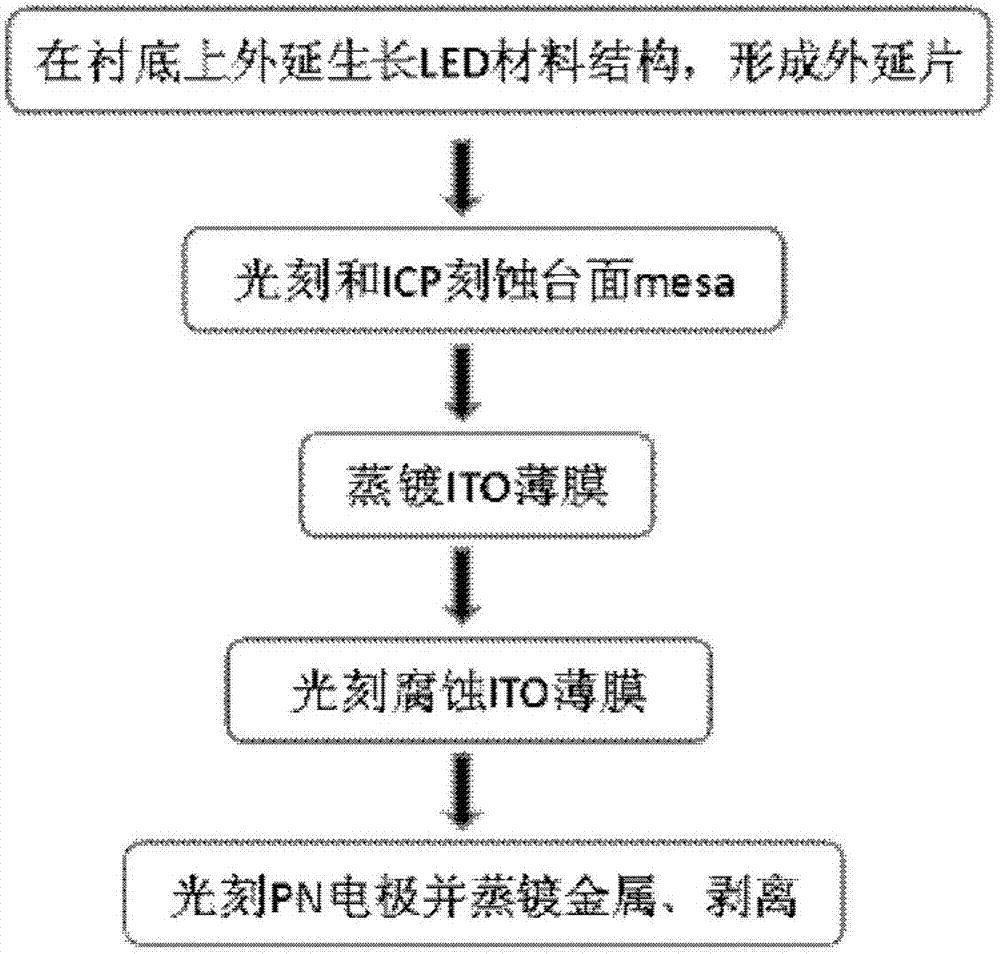
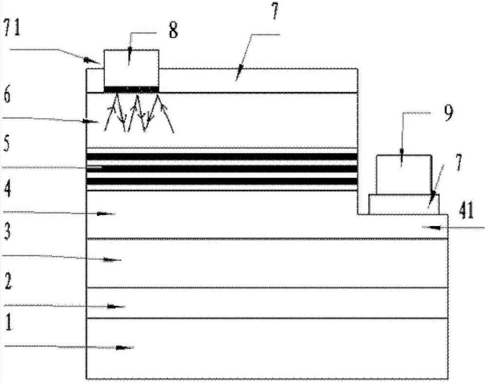
[0018] see figure 1 and figure 2 As shown, the present invention provides a method for manufacturing a GaN-based LED chip that improves brightness, comprising the steps of:

[0019] Step 1: Take a semiconductor substrate 1, the material of the semiconductor substrate 1 is sapphire, silicon, silicon carbide or metal;

[0020] Step 2: Using metal-organic chemical vapor deposition (MOCVD), sequentially grow a low-temperature GaN buffer layer 2 (with a thickness of 1 μm), an undoped GaN layer 3 (with a thickness of 1 μm), and an N-GaN layer on the semiconductor substrate 1 4 (thickness is 3 μm), multi-quantum well light-emitting layer 5 (thickness is 150nm) and mP-GaN layer 6 (thickness is 300n), forms GaN epitaxial wafer, wherein said semiconductor substrate 1 is sapphire, silicon, silicon carbide or Metal;

[0021] Step 3: Etching downward on one side of the surface of the GaN epitaxial wafer, the etching depth reaches the N-GaN layer 4 , and forming a mesa 41 on one side o...


PUM


Abstract

The invention discloses a method for manufacturing a brightness-improved GaN-based light emitting diode (LED) chip. The method comprises the following steps of: 1, taking a semiconductor substrate; 2, sequentially growing a low-temperature GaN buffer layer, a non-doped GaN layer, an N-GaN layer, a multi-quantum well light emitting layer and a P-GaN layer on the semiconductor substrate by adopting a metal organic chemical vapor deposition method to form a GaN epitaxial sheet; 3, performing downward etching on one side of the surface of the GaN epitaxial sheet till reaching the N-GaN layer, and forming a mesa on one side of the N-GaN layer; 4, performing vapor deposition on the upper surface of the GaN epitaxial sheet to form an indium tin oxide (ITO) film; 5, photo-etching a groove on the ITO film on the P-GaN layer, corroding the ITO film on the side walls of the multi-quantum well light emitting layer and the P-GaN layer, and reserving the ITO film on the mesa; and 6, manufacturing a P electrode in the groove on the ITO film, manufacturing an N electrode on the ITO film on the mesa, and thus obtaining the GaN-based LED chip.

Description

technical field [0001] The invention relates to the field of photoelectric devices, in particular to a method for manufacturing a GaN-based LED chip with improved brightness. Background technique [0002] A light emitting diode (LED) is a junction electroluminescent semiconductor device that converts electrical signals into optical signals. Once GaN-based LEDs appeared as solid-state light sources, they were widely praised for their high efficiency, long life, and environmental protection. Solid-state lighting using LEDs as new light sources will have the opportunity to gradually replace traditional lighting and enter the homes of ordinary people. [0003] Epitaxial wafers of sapphire substrates are generally used to prepare high-brightness GaN-based LEDs. How to improve the luminous efficiency of GaN-based LEDs has been the focus of research (see Figure 5 , Figure 5 is a schematic diagram of the structure of a conventional GaN-based LED). At present, the internal quantu...

Claims


Application Information

Patent Timeline
IPC IPC(8): H01L33/36H01L33/00
Inventor 李璟王国宏詹腾孔庆峰
Owner INST OF SEMICONDUCTORS - CHINESE ACAD OF SCI
Why Eureka
Try Eureka