Two-dimensional silicon substrate photonic crystal line-defect slow optical waveguide device

A technology of photonic crystals and waveguide devices, applied in light guides, optics, optical components, etc., can solve problems that have not been reported in the past, and achieve the effects of good signal fidelity, high efficiency, and high group refractive index

Inactive Publication Date: 2013-06-26
QINGDAO UNIV
View PDF3 Cites 6 Cited by
  • Summary
  • Abstract
  • Description
  • Claims
  • Application Information

AI Technical Summary

Problems solved by technology

[0003] The uniaxially symmetrical scattering element is a new development of the photonic crystal structure. In order to optimize the relationship between the forbidden band and slow light, the uniaxially symmetrical scattering element increases the structural parameters of the scattering element and breaks its original symmetrical scattering element mode. Changing the structure from biaxial symmetry to uniaxial symmetry, research in this area has not yet been reported

Method used


Image

  • Two-dimensional silicon substrate photonic crystal line-defect slow optical waveguide device
  • Two-dimensional silicon substrate photonic crystal line-defect slow optical waveguide device
  • Two-dimensional silicon substrate photonic crystal line-defect slow optical waveguide device

Examples


Embodiment

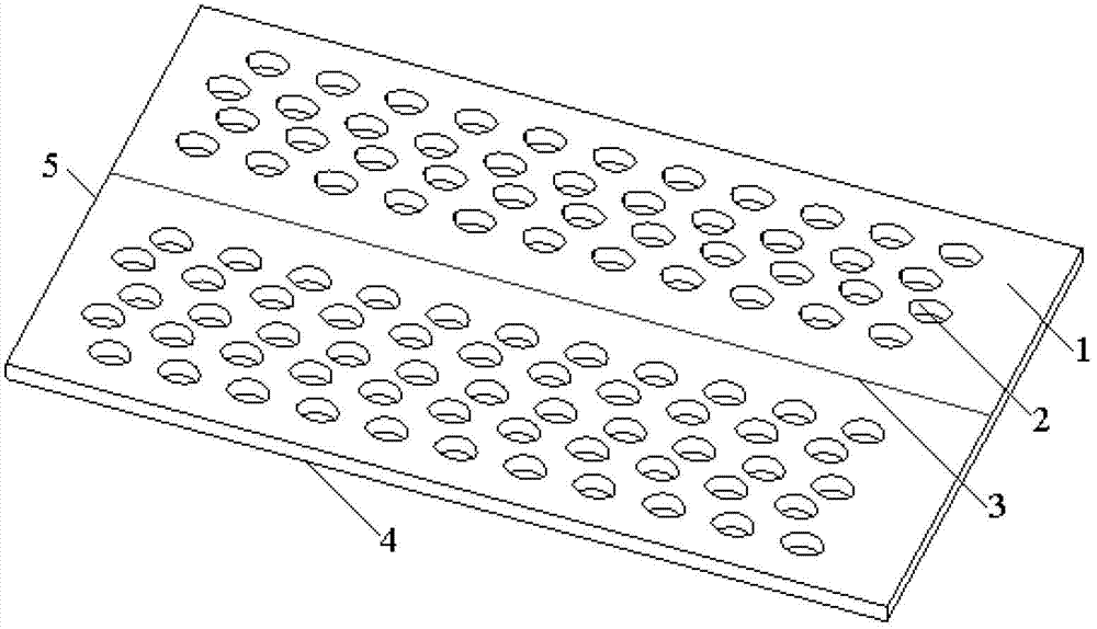
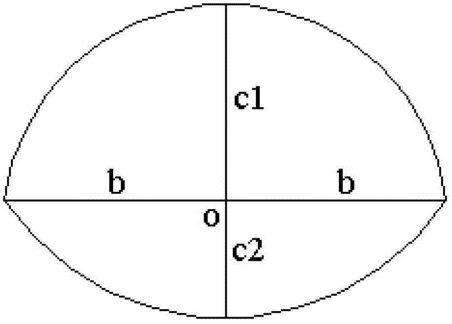
[0019] The main structure of this implementation includes a two-dimensional silicon wafer 1, a uniaxially symmetrical circular segment scattering element 2, a line defect 3, a long side 4 of the silicon wafer, and a short side 5 of the silicon wafer; Along the direction of the long side 4 of the two-dimensional silicon wafer 1, there are 6-10 rows of uniaxially symmetrical circular bow-shaped scattering elements 2 with the centerline of the two-dimensional silicon wafer as the axis of symmetry, and the symmetrical axis of the two-dimensional silicon wafer 1 There is a row of line defects 3 formed by unetched circular segment scattering elements; 90-100 uniaxially symmetrical circular segment scattering elements 2 are equally spaced on each row of uniaxially symmetrical circular segment scattering elements 2; The center of the uniaxially symmetrical circular segment scattering element 2 is arranged in an equilateral hexagon on the surface of the two-dimensional silicon wafer 1, ...


PUM


Abstract

The invention belongs to the technical field of optical equipment manufacturing, and relates to a two-dimensional silicon substrate photonic crystal line-defect slow optical waveguide device. Monosymmetrical circular-segment-shaped scattering elements are sequentially arranged and etched on the surface of a two-dimensional silicon wafer along the direction of the long edge of the two-dimensional silicon wafer, and a row of positions at which no monosymmetrical circular-segment-shaped scattering element is etched is left at a symmetric axis of the two-dimensional silicon wafer so as to form a line defect; the centers of adjacent monosymmetrical circular-segment-shaped scattering elements are arranged in the shape of an equilateral hexagon on the surface of the two-dimensional silicon wafer, and each monosymmetrical circular-segment-shaped scattering element is formed by docking two semicircular segments; the digged monosymmetrical circular-segment-shaped scattering elements respectively and sequentially arranged on the two-dimensional silicon wafer are of a transparent structure; and the direction of the line defect is parallel to the direction of a long axis of the monosymmetrical circular-segment-shaped scattering element. The two-dimensional silicon substrate photonic crystal line-defect slow optical waveguide device is simple in structure, small in size, low in cost, high in stability, high in efficiency, simple and feasible, high in group refractive index, large in slow optical bandwidth and good in signal fidelity, and can be widely applied to the technical field of solar photovoltaic conversion and photonic crystal luminescence.

Description

Technical field: [0001] The invention belongs to the technical field of optical equipment manufacturing, and relates to a two-dimensional silicon-based photonic crystal line-defect slow light waveguide structure composed of high-group refractive index, uniaxial symmetry, and circular bow-shaped scattering elements, in particular to a two-dimensional silicon-based photonic crystal Line defect slow light waveguide devices. Background technique: [0002] The slow light effect is that electromagnetic waves have a group velocity much lower than the speed of light. The photonic crystal slow light structure has incomparable advantages in practical applications due to its small and compact structure, low transmission loss and room temperature operation. Existing photonic crystal slow optical waveguides mainly have two forms: line-defect waveguides and point-defect coupled waveguides. In line-defect waveguides, the group velocity of light waves is generally larger, but the dispersion...

Claims


Application Information

Patent Timeline
Patent Type & Authority Applications(China)
IPC IPC(8): G02F1/365G02F1/355G02B6/122
Inventor 万勇戈升波刘培晨郭月贾明辉
Owner QINGDAO UNIV
Why Eureka
Try Eureka