Check patentability & draft patents in minutes with Patsnap Eureka AI!

Ultra-high voltage LDMOS (Laterally Diffused Metal Oxide Semiconductor) device structure and production method thereof

A device structure and ultra-high voltage technology, which is applied in semiconductor/solid-state device manufacturing, semiconductor devices, electrical components, etc., can solve the problems of difficult to weaken the surface electric field in the drift region and the device is easy to be broken down, so as to increase the process steps and cost, The effect of increasing the breakdown voltage

Active Publication Date: 2013-06-26
SHANGHAI HUAHONG GRACE SEMICON MFG CORP
View PDF6 Cites 13 Cited by
  • Summary
  • Abstract
  • Description
  • Claims
  • Application Information

AI Technical Summary

Problems solved by technology

However, since the edge of the field oxygen is where the electric field is concentrated, the surface electric field under the bird's beak of LOCOS (local oxide silicon) is the strongest, and the field plate above the field oxygen of the LDMOS polycrystalline extension to the drift region is difficult to weaken the drift region. The surface electric field, at this time, the N-type impurities under the LOCOS bird's beak are difficult to be exhausted, so the breakdown voltage will become smaller, and the device will be easily broken down

Method used


Image

  • Ultra-high voltage LDMOS (Laterally Diffused Metal Oxide Semiconductor) device structure and production method thereof
  • Ultra-high voltage LDMOS (Laterally Diffused Metal Oxide Semiconductor) device structure and production method thereof
  • Ultra-high voltage LDMOS (Laterally Diffused Metal Oxide Semiconductor) device structure and production method thereof

Examples


Embodiment Construction

[0018] In order to have a more specific understanding of the technical content, characteristics and effects of the present invention, now taking the ultra-high voltage N-type LDMOS device as an example, combined with the illustrated embodiment, the technical solution of the present invention is described in detail as follows:

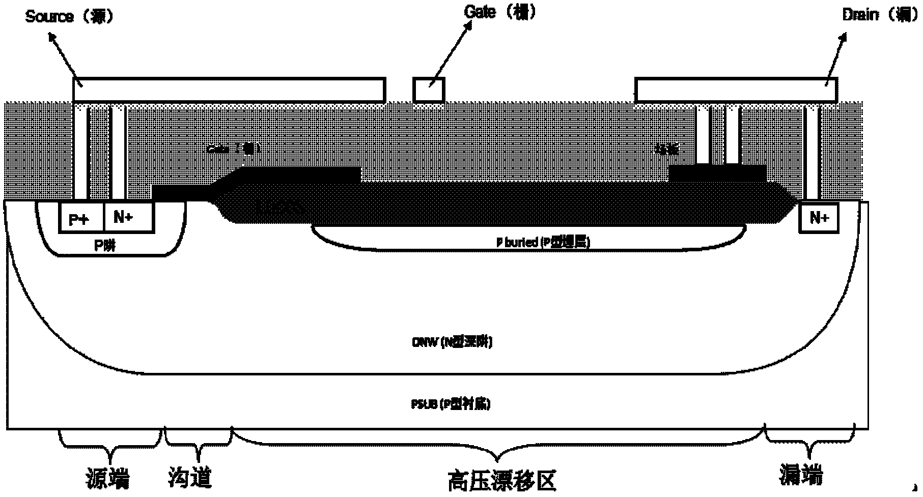
[0019] Such as image 3 As shown, the ultra-high-voltage LDMOS device of the embodiment of the present invention has two N-type deep wells (DNW), wherein, a P well (PW) for the source end of the LDMOS device is placed in one DNW, and a drain end withstand voltage is placed in the other DNW. The P-type buried layer (P buried); the two deep N wells are separated by a P-type substrate (PSUB).

[0020] The preparation method of the ultra-high voltage LDMOS device with the above structure is as follows:

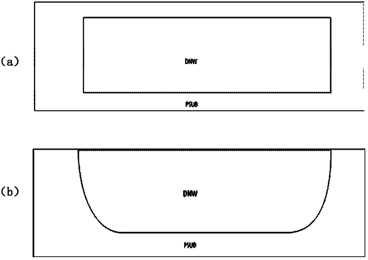
[0021] Step 1, design the mask plate of the DNW of the LDMOS device, and inject the traditional DNW into the pattern (such as figure 2 shown) changed to...


PUM


Abstract

The invention discloses an ultra-high voltage LDMOS (Laterally Diffused Metal Oxide Semiconductor) device structure which comprises a source terminal, a drain terminal, a high voltage drift region and a grid electrode channel. The source terminal is provided with a substrate trap; a surface of the high voltage drift region is provided with an inversion layer; two physically connected deep traps which are respectively used for placing the substrate trap and the inversion layer are also designed in an LDMOS; and a gap between the two deep traps is located near an LOCOS (Local Oxidation of Silicon) bird beak. The invention also discloses a production method of the ultra-high voltage LDMOS device structure. The production method of the ultra-high voltage LDMOS device structure comprises process steps such as designing mask blanks of the deep traps, performing photoetching, performing ion implantation, removing of photoresist and performing hot-push of traps. The ultra-high voltage LDMOS device structure and the production method of the ultra-high voltage LDMOS device structure have the advantages of improving electric field distribution near LOCOS, reducing peak electric fields, achieving the balance of N type charge and P type charge and achieving the purpose of improvement of a reverse breakdown voltage of a device on the basis of increasing no process step and cost due to the facts that a deep trap of the source terminal and a deep trap of the high voltage drift region are separated and are connected together through push-trap after the ion implantation and the gap of the deep traps is located under the LOCOS bird beak.

Description

technical field [0001] The invention relates to the field of semiconductor integrated circuit manufacturing, in particular to the structure and preparation process of an ultra-high voltage LDMOS device. Background technique [0002] The ultra-high voltage LDMOS device (laterally diffused metal oxide semiconductor, laterally diffused metal oxide semiconductor transistor) is a power device with a double-diffused structure, and its structure is as follows figure 1 shown. This technology is to implant twice in the same source / drain region, one implantation of arsenic (As) with a higher concentration, and the other implantation of boron (B) with a lower concentration, and then a high-temperature push process after the implantation, due to the diffusion of boron It is faster than arsenic, so it will diffuse farther along the lateral direction under the gate boundary, forming a channel with a concentration gradient - P well (PW), and the channel length is determined by the differe...

Claims


Application Information

Patent Timeline
IPC IPC(8): H01L29/06H01L29/78H01L21/336
CPCH01L29/063H01L29/1083H01L29/402H01L29/42368H01L29/7816H01L29/7835
Inventor 宁开明董科马栋朱东园
Owner SHANGHAI HUAHONG GRACE SEMICON MFG CORP
Features
  • R&D
  • Intellectual Property
  • Life Sciences
  • Materials
  • Tech Scout
  • Unparalleled Data Quality
  • Higher Quality Content
  • 60% Fewer Hallucinations
Learn More