Method for improving voltage withstanding performance of MIS-HEMT and MIS-HEMT

A technology of MIS-HEMT and process method, applied in the field of semiconductor device manufacturing process, can solve the problems of large epitaxy defects, unfavorable application of high-density integrated circuits, and increase of device area

Inactive Publication Date: 2018-01-23
PEKING UNIV SHENZHEN GRADUATE SCHOOL
View PDF3 Cites 2 Cited by
  • Summary
  • Abstract
  • Description
  • Claims
  • Application Information

AI Technical Summary

Problems solved by technology

[0003] At present, the GaN wafers used are epitaxially grown by MOCVD or MBE, the growth process is immature, and the epitaxy defects are large, which leads to a large gap between the actual withstand voltage of HEMT devices and the theoretical withstand voltage
At present, the vertical withstand voltage of AlGaN / GaN devices is generally optimized by epitaxial doping or the deposition of high-resistance film layers; while the lateral withstand voltage problem is generally solved by expanding the gate (Gate) and the drain (Drain) The distance between them is improved, which undoubtedly increases the area of ​​the device, which is not conducive to the application of high-density integrated circuits; in addition, sometimes a vertical vertical device structure is used to convert the total withstand voltage of the device into the vertical withstand voltage of the device , so as to improve the pressure resistance of the device by changing the film layer structure and thickness of the material, which can ensure the miniaturization of the lateral size of the device, but this technology has high process requirements and low repeatability, and is not suitable for large-scale production. Produce

Method used


Image

  • Method for improving voltage withstanding performance of MIS-HEMT and MIS-HEMT
  • Method for improving voltage withstanding performance of MIS-HEMT and MIS-HEMT
  • Method for improving voltage withstanding performance of MIS-HEMT and MIS-HEMT

Examples


Embodiment Construction

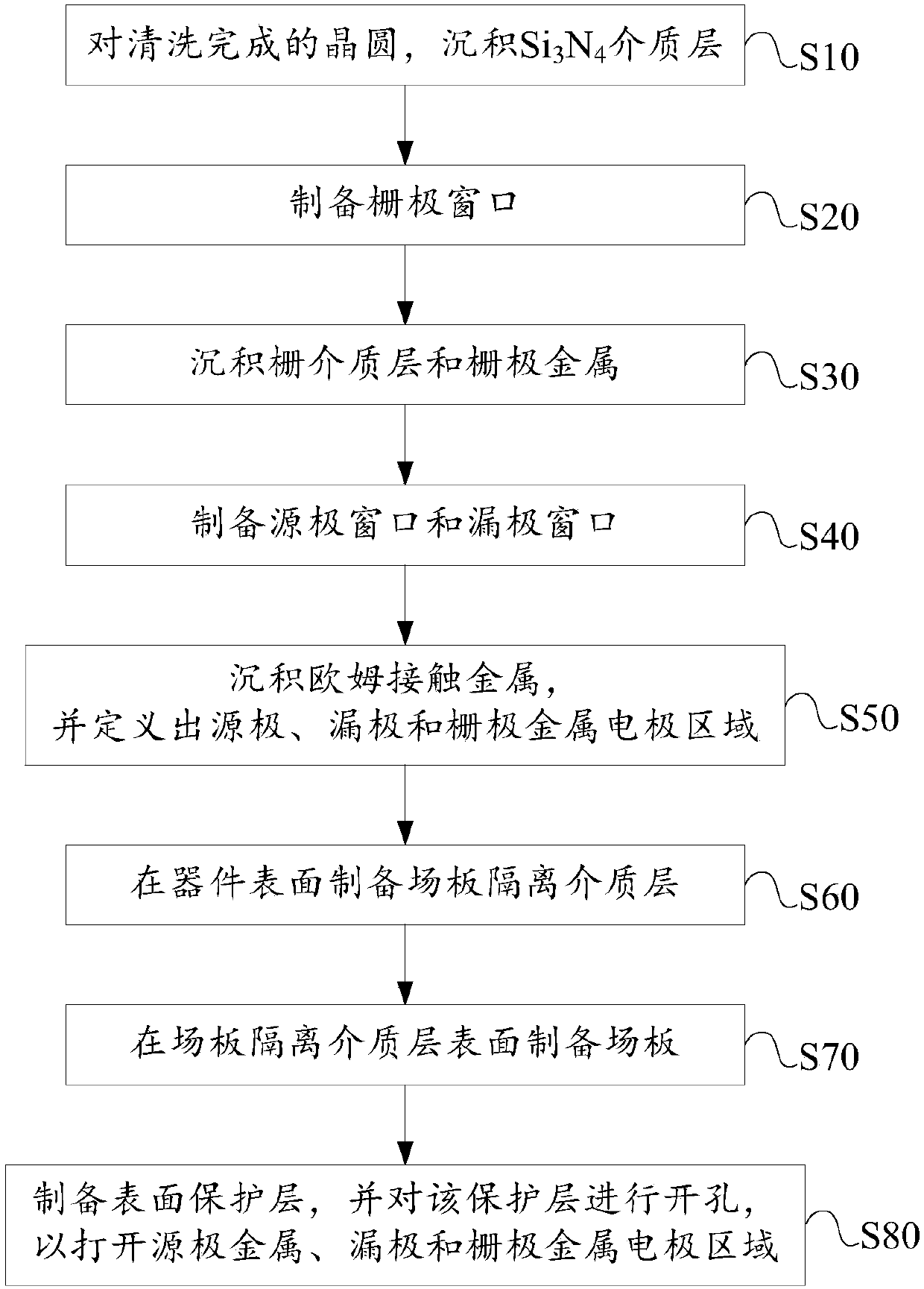
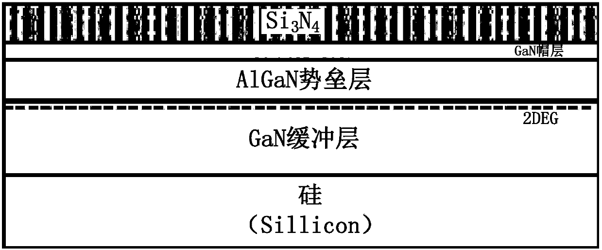
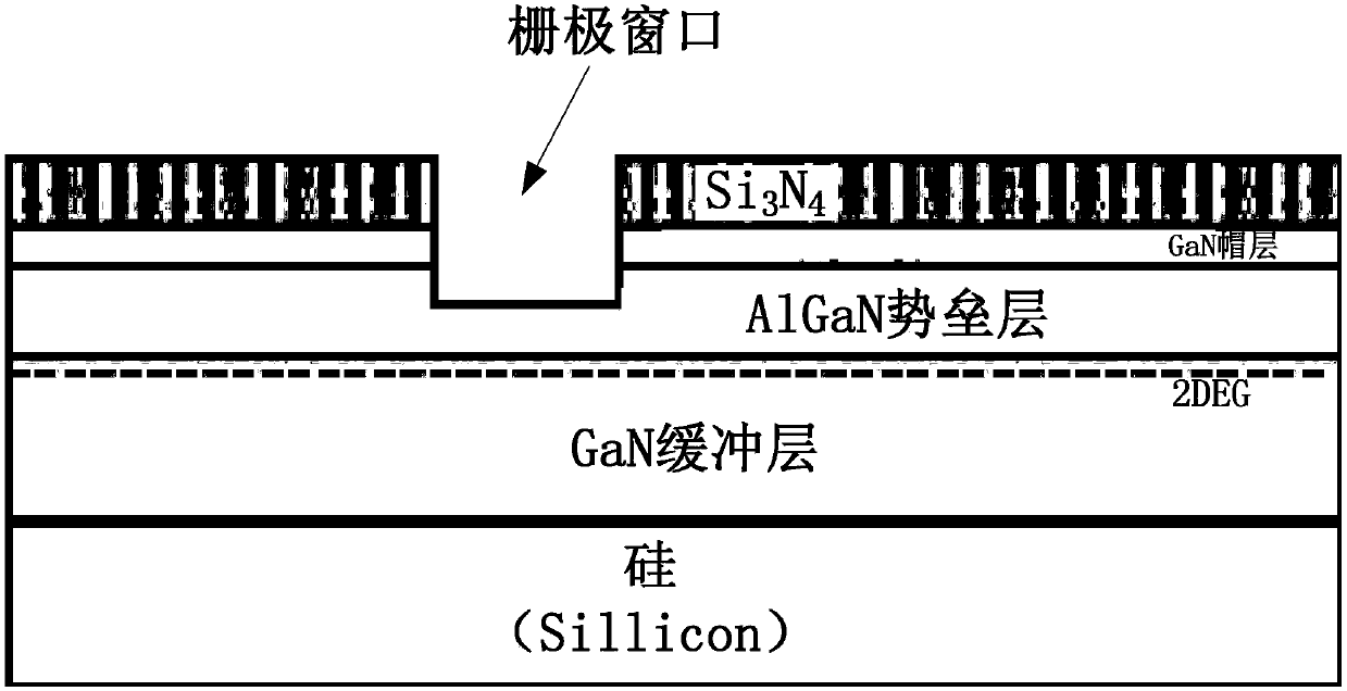
[0043] The present invention will be further described in detail below through specific embodiments in conjunction with the accompanying drawings. Wherein, similar elements in different embodiments adopt associated similar element numbers. In the following embodiments, many details are described in order to enable the application to be better understood. However, those skilled in the art can easily recognize that some of the features can be omitted in different situations, or can be replaced by other elements, materials, and methods. In some cases, some operations related to the application are not shown or described in the description, this is to avoid the core part of the application being overwhelmed by too many descriptions, and for those skilled in the art, it is necessary to describe these operations in detail Relevant operations are not necessary, and they can fully understand the relevant operations according to the description in the specification and general technic...


PUM


Abstract

The invention provides a method for improving voltage withstanding performance of a MIS-HEMT and the MIS-HEMT. The method comprises the following steps: for a cleaned wafer, depositing a Si3N4 dielectric layer; preparing a gate window; depositing a gate dielectric layer and gate metal; preparing a source window and a drain window; depositing ohm contact metal, and defining a source metal electrodearea, a drain metal electrode area and a gate metal electrode area; preparing a field plate isolation medium layer on the surface of the device; preparing a field plate on the surface of the field plate isolation medium layer; and preparing a surface protecting layer, and carrying out trepanning on the protecting layer to open the source metal electrode area, the drain metal electrode area and the gate metal electrode area. By introducing the field plate between a gate and a drain, electric field distribution in a channel is changed, and peak electric filed between the gate and the drain is reduced, thereby achieving a purpose of improving and increasing the voltage withstanding performance of the MIS-HEMT.

Description

technical field [0001] The invention relates to a manufacturing process of a semiconductor device, in particular to a process method for improving the withstand voltage characteristics of an MIS-HEMT and the MIS-HEMT. Background technique [0002] The III-V wide bandgap compound semiconductor material represented by gallium nitride GaN has the characteristics of high breakdown electric field, high electron saturation, high drift rate and high thermal conductivity, so it is very suitable for preparing high-power, high-speed and large-scale Voltage power electronic devices. AlGaN / GaN MIS-HEMT, as the most attractive device type, benefits from the extremely strong spontaneous polarization and piezoelectric polarization effects between GaN and AlGaN on the one hand, which makes GaN / AlGaN form a high electron concentration And two-dimensional electron gas (2-DEG) with high electron mobility, the electron concentration is as high as 10 12 -10 13 cm -2 , the electron mobility c...

Claims


Application Information

Patent Timeline
Patent Type & Authority Applications(China)
IPC IPC(8): H01L29/778H01L29/40H01L21/335
Inventor 孙辉刘美华林信南陈东敏
Owner PEKING UNIV SHENZHEN GRADUATE SCHOOL
Why Eureka
Try Eureka