Lateral transistor with AlGaN/GaN heterojunction and production method of lateral transistor

A technology of lateral transistors and heterojunctions, applied in semiconductor/solid-state device manufacturing, semiconductor devices, electrical components, etc., to improve performance and optimize vertical electric field

Active Publication Date: 2019-06-14
XIDIAN UNIV
View PDF5 Cites 2 Cited by
  • Summary
  • Abstract
  • Description
  • Claims
  • Application Information

AI Technical Summary

Problems solved by technology

However, since the nitride material has no natural substrate, it is necessary

Method used


Image

  • Lateral transistor with AlGaN/GaN heterojunction and production method of lateral transistor

Examples


Embodiment Construction

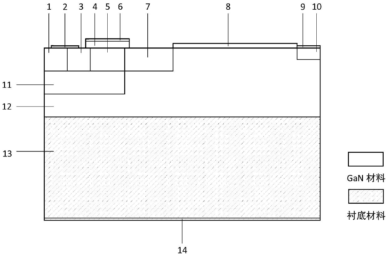
[0037] The present invention will be described below by taking an N-channel lateral transistor with an AlGaN / GaN heterojunction as an example in conjunction with the accompanying drawings.

[0038] Such as figure 1 Shown, the characteristic of the structure of the present embodiment is:

[0039] Base region, source region and channel substrate contact formed by ion implantation based on one end of the GaN epitaxial layer; drain region formed by ion implantation based on the other end of the GaN epitaxial layer; the region of the GaN epitaxial layer close to the base region by ion implantation An N-type drift region is formed by implantation, and the remaining region of the GaN epitaxial layer (between the N-type drift region and the drain region) is formed with an AlGaN layer by heteroepitaxial growth. The length of the AlGaN / GaN heterojunction is 3-3 times the length of the N-type drift region. 10 times; the GaN epitaxial layer under the base region and the source region is ...


PUM

PropertyMeasurementUnit
Thicknessaaaaaaaaaa
Thicknessaaaaaaaaaa

Abstract

The invention provides a lateral transistor with an AlGaN/GaN heterojunction and a production method of the lateral transistor. A part of a drift region of the device is the AlGaN/GaN heterojunction.The AlGaN/GaN heterojunction forms a high-density two-dimensional electron gas (2DEG) at a heterojunction interface through spontaneous polarization and piezoelectric polarization effects, the 2DEG has a high migration rate in a heterojunction conducting channel, and therefore the lateral transistor provided with the AlGaN/GaN heterojunction has low conduction resistance. When the device is switched off, the 2DEG is exhausted, meanwhile a new electric field peak is introduced into the surface of the device, and therefore a peak electric field at a grid edge of the device is lowered. A galliumnitride material is formed through epitaxy on a substrate material, the heterojunction between a gallium nitride epitaxial layer and a substrate optimizes longitudinal electric field distribution of the transistor, and therefore the breakdown voltage of the device is increased.

Description

technical field [0001] The invention relates to the field of power semiconductor devices, in particular to a lateral transistor with an AlGaN / GaN heterojunction. Background technique [0002] Transverse field effect transistors have the advantages of easy integration, good thermal stability, good frequency stability, low power consumption, multi-subconduction, small power drive, and high switching speed. They are the core of intelligent power circuits and high-voltage devices. Due to the growing market demand for portable power management and automotive electronics, it is receiving increasing attention across the globe. [0003] Wide bandgap semiconductor materials have the characteristics of large bandgap width, high electron drift saturation velocity, small dielectric constant, and good electrical conductivity. GaN materials have excellent properties and potential applications in the field of power devices. One of the cores of the third-generation semiconductor materials,...

Claims


Application Information

Patent Timeline
IPC IPC(8): H01L29/778H01L29/06H01L21/335
Inventor 段宝兴王彦东黄芸佳杨银堂
Owner XIDIAN UNIV
Why Eureka
Try Eureka