Vapor plating method for organic light-emitting display

An organic and evaporation technology, which is applied in vacuum evaporation coating, sputtering coating, electric solid devices, etc., can solve the problems that the substrate cannot be reached, and achieve the effect of improving the service life, increasing the utilization rate, and avoiding the deformation of the board surface

Inactive Publication Date: 2013-07-17
KUN SHAN POWER STENCIL
View PDF2 Cites 1 Cited by
  • Summary
  • Abstract
  • Description
  • Claims
  • Application Information

AI Technical Summary

Problems solved by technology

[0014] The technical problem to be solved by the present invention is that in the existing OLED manufacturing technology, the organic particles cannot reach the substrate due to the shielding of the opening wall during evaporation. It provides a new organic light-emitting semiconductor evaporation method, which has organic The advantages of high material utilization rate, high film formation rate, long service life of mask plate and cost saving

Method used


Image

  • Vapor plating method for organic light-emitting display
  • Vapor plating method for organic light-emitting display
  • Vapor plating method for organic light-emitting display

Examples


Embodiment 1

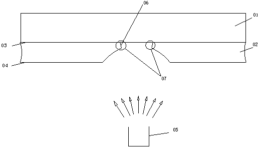
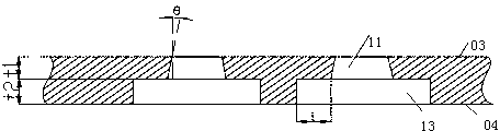
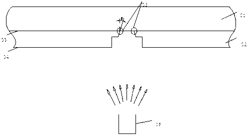
[0035] An organic light-emitting semiconductor evaporation method, comprising the following steps: combining the ITO surface of a mask plate for evaporation with the ITO semiconductor glass surface, and corresponding the evaporation surface of the mask plate to an organic evaporation source; evaporating organic materials, making The organic material is attached to the surface of the ITO semiconductor glass through the opening on the mask plate; the mask plate and the ITO semiconductor glass are separated to complete the evaporation; wherein, the shape of the mask plate is a quadrilateral metal plate, and the mask plate has an ITO surface Layer and evaporation surface layer two-layer structure, the mask plate has an opening through the ITO surface layer and the evaporation surface layer, the opening size of the ITO surface layer is smaller than the opening size of the evaporation surface layer, along the thickness direction of the mask plate In the transverse section, the shape ...

Embodiment 2

[0039] An organic light-emitting semiconductor evaporation method, comprising the following steps: combining the ITO surface of a mask plate for evaporation with the ITO semiconductor glass surface, and corresponding the evaporation surface of the mask plate to an organic evaporation source; evaporating organic materials, making The organic material is attached to the surface of the ITO semiconductor glass through the opening on the mask plate; the mask plate and the ITO semiconductor glass are separated to complete the evaporation; wherein, the mask plate is a rectangular Invar alloy plate metal plate, the The mask plate has a two-layer structure of an ITO surface layer and an evaporation surface layer. The mask plate has an opening through the ITO surface layer and the evaporation surface layer. The opening size of the ITO surface layer is smaller than the opening size of the evaporation surface layer. Along the mask On the transverse section in the thickness direction of the...

Embodiment 3

[0044] An organic light-emitting semiconductor evaporation method, comprising the following steps: combining the ITO surface of a mask plate for evaporation with the ITO semiconductor glass surface, and corresponding the evaporation surface of the mask plate to an organic evaporation source; evaporating organic materials, making The organic material is attached to the surface of the ITO semiconductor glass through the opening on the mask plate; the mask plate and the ITO semiconductor glass are separated to complete the evaporation; wherein, the mask plate is a mask plate for evaporation, and the shape is a rectangular nickel-cobalt alloy The metal plate, the mask plate has a two-layer structure of an ITO surface layer and an evaporation surface layer, and the mask plate has an opening through the ITO surface layer and the evaporation surface layer, and the opening size of the ITO surface layer is smaller than that of the evaporation surface layer. The size of the opening, on t...


PUM

PropertyMeasurementUnit
thicknessaaaaaaaaaa
thicknessaaaaaaaaaa
thicknessaaaaaaaaaa

Abstract

The invention relates to a vapor plating method for an organic light-emitting semiconductor, and aims to mainly solve the technical problem that organic particles cannot reach a substrate due to shadowing of a mask plate aperture wall during vapor plating in the existing OLED (organic light-emitting diode) manufacturing technologies. The invention employs a vapor plating method for an organic light-emitting semiconductor. The mask plate for vapor plating is a quadrangular metal plate, and has a two-layer structure composed of an ITO surface layer and a vapor plating surface layer. The mask plate is equipped with apertures running through the ITO surface layer and the vapor plating surface layer. The size of the apertures on the ITO surface layer is smaller than that on the vapor plating surface layer, and on a cross section of the mask plate in the thickness direction, the aperture shape is a trapezoid. According to the technical scheme, the problem is well solved. Thus, the method can be used in the industrial production of organic light-emitting diodes.

Description

[0001] technical field [0002] The invention relates to an organic light-emitting semiconductor vapor deposition method in the OLED manufacturing process. Background technique [0003] Generally, an OLED device is an emissive display device that emits light by electrically exciting a fluorescent organic compound. The OLED device can be regarded as a passive matrix OLED (PMOLED) device or an active matrix OLED (AMOLED) device according to a driving manner of N×M pixels that can be arranged in a matrix. Compared with PMOLED devices, AMOLED devices are suitable for large-sized displays due to their low power consumption and high resolution. [0004] Depending on the direction in which light is emitted from the organic compound, the OLED device can be a top-emitting OLED device, a bottom-emitting OLED device, or a top and bottom-emitting OLED device. Top-emitting OLED devices emit light in the opposite direction to the substrate on which the pixels are disposed and, unlike bo...

Claims


Application Information

Patent Timeline
Patent Type & Authority Applications(China)
IPC IPC(8): C23C14/04C23C14/24H01L51/56
Inventor 魏志凌高小平郑庆靓
Owner KUN SHAN POWER STENCIL
Why Eureka
Try Eureka