Method for making line in direct negative etching way

A production method and direct technology, applied in the direction of removing conductive materials by chemical/electrolytic methods, etc., can solve the problems of unsuitability for mass production, long production process time, large copper usage, etc., to save surface treatment costs and operation. The effect of simplifying and avoiding contamination

Active Publication Date: 2013-07-17
WESKY SUINING ELECTRONICS
View PDF5 Cites 18 Cited by
  • Summary
  • Abstract
  • Description
  • Claims
  • Application Information

AI Technical Summary

Problems solved by technology

This patented process takes a long time, requires two exposures and developments, wet film printing and tin plating, and a large amount of copper is used. This method is not only complicated in process, but also high in production cost, and is not suitable for mass production.
[0006] To sum up, the existing negative film etching circuit manufacturing method has the problems of long production process time, low production efficiency, tin plating, tin waste liquid treatment, high investment cost, and serious environmental pollution.

Method used


Image

  • Method for making line in direct negative etching way
  • Method for making line in direct negative etching way

Examples


Embodiment 1

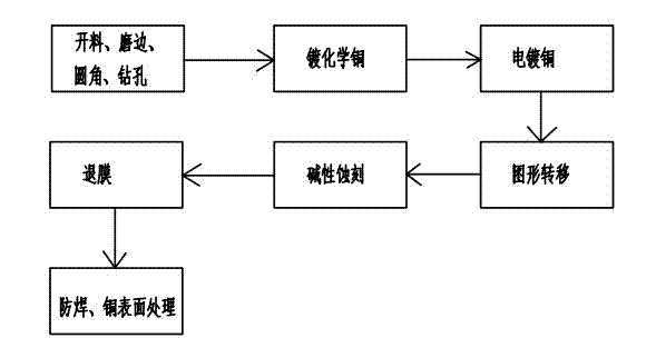
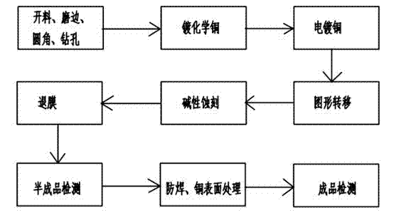
[0041] A method for directly etching a circuit on a negative film, comprising the following steps:

[0042] A. Carry out material cutting, edge grinding, filleting and drilling on the PCB substrate in sequence;

[0043] B. After step A, firstly plate chemical copper on the entire PCB substrate, the thickness of chemical copper is 0.5um; then electroplate copper on the PCB substrate, the thickness of electroplated copper is 18um;

[0044] C. After step B, the PCB substrate surface is subjected to graphic transfer, and the graphic transfer includes lamination, one-time exposure and development treatment; the one-time exposure refers to the one-time exposure of the electroplated copper on the laminated PCB substrate surface by using line film. ; After exposure, the graphics transfer is completed through development treatment;

[0045] D. After step C, the PCB substrate is subjected to alkaline etching treatment, until the pH value of the PCB substrate is 8;

[0046] E. After th...

Embodiment 2

[0069] A method for directly etching a circuit on a negative film, comprising the following steps:

[0070] A. Carry out material cutting, edge grinding, filleting and drilling on the PCB substrate in sequence;

[0071] B. After step A, firstly plate chemical copper on the entire PCB substrate, the thickness of chemical copper is 0.8um; then electroplate copper on the PCB substrate, the thickness of electroplated copper is 20um;

[0072] C. After step B, the PCB substrate surface is subjected to graphic transfer, and the graphic transfer includes lamination, one-time exposure and development treatment; the one-time exposure refers to the one-time exposure of the electroplated copper on the laminated PCB substrate surface by using line film. ; After exposure, the graphics transfer is completed through development treatment;

[0073] D. After step C, the PCB substrate is subjected to alkaline etching treatment, until the pH value of the PCB substrate is 8;

[0074] E. After th...

Embodiment 3

[0087] A method for directly etching a circuit on a negative film, comprising the following steps:

[0088] A. Carry out material cutting, edge grinding, filleting and drilling on the PCB substrate in sequence;

[0089] B. After step A, firstly plate chemical copper on the entire PCB substrate, the thickness of chemical copper is 1um; then electroplate copper on the PCB substrate, the thickness of electroplated copper is 25um;

[0090] C. After step B, the PCB substrate surface is subjected to graphic transfer, and the graphic transfer includes lamination, one-time exposure and development treatment; the one-time exposure refers to the one-time exposure of the electroplated copper on the laminated PCB substrate surface by using line film. ; After exposure, the graphics transfer is completed through development treatment;

[0091] D. After step C, the PCB substrate is subjected to alkaline etching treatment, until the pH value of the PCB substrate is 9;

[0092] E. After the ...


PUM


Abstract

The invention discloses a method for making a line in a direct negative etching way. The method comprises the steps of: cutting, edging, corner rounding and drilling; plating of chemical copper; electroplating of copper; pattern transfer; alkaline etching; film removal; and solder masking and copper surface treatment. Exposure is adopted only once, the technical problem that the conventional negative is required to be exposed and developed twice is solved, production flow time is shortened, and production efficiency is improved; in addition, tin is not required to be plated, so that the treatment of tin waste liquor is eliminated, and cost is saved; and moreover, the method is environment-friendly and applicable to batch production.

Description

technical field [0001] The invention relates to the field of circuit production, in particular to a method for producing a circuit by direct etching of a negative film of copper on a board surface. Background technique [0002] At present, when the circuit board is making the circuit, it is only necessary to have copper in the hole and copper in the line. Due to the influence of the electroplating solution on the dry film, it will be permeated, etched and short-circuited. The roughness of the hole is large and there will be holes without copper. It is difficult to ensure the uniformity of copper and hole copper, high-speed signal transmission lines, and the width of the line is difficult to guarantee. [0003] The existing positive film cannot be made of fine lines due to the high requirement of copper thickness uniformity. [0004] Negative film (Negatave): Refers to the pattern of the conductor circuit on various negative films (such as black and white film, brown film) i...

Claims


Application Information

Patent Timeline
Patent Type & Authority Applications(China)
IPC IPC(8): H05K3/06
Inventor 陈胜平罗献军
Owner WESKY SUINING ELECTRONICS
Why Eureka
Try Eureka