Conductive hard carbon film, and film forming method therefor

一种硬质碳膜、成膜方法的技术,应用在电路、放电管、电气元件等方向,能够解决品质参差不齐、探头基材耐磨损性不充分、检查结果不稳定等问题,达到稳定体积电阻率和硬度的效果

Active Publication Date: 2013-07-17
NOMURA PLATING CO LTD
View PDF9 Cites 7 Cited by
  • Summary
  • Abstract
  • Description
  • Claims
  • Application Information

AI Technical Summary

Problems solved by technology

The result is variable quality due to erratic inspection results
[0004] (2) The wear resistance of the probe base material is insufficient, and the probe needs to be replaced frequently
Thus, since there is inherently a trade-off relationship between hardness and conductivity, it is not easy to balance hardness and conductivity

Method used


Image

  • Conductive hard carbon film, and film forming method therefor
  • Conductive hard carbon film, and film forming method therefor
  • Conductive hard carbon film, and film forming method therefor

Examples


Embodiment 1

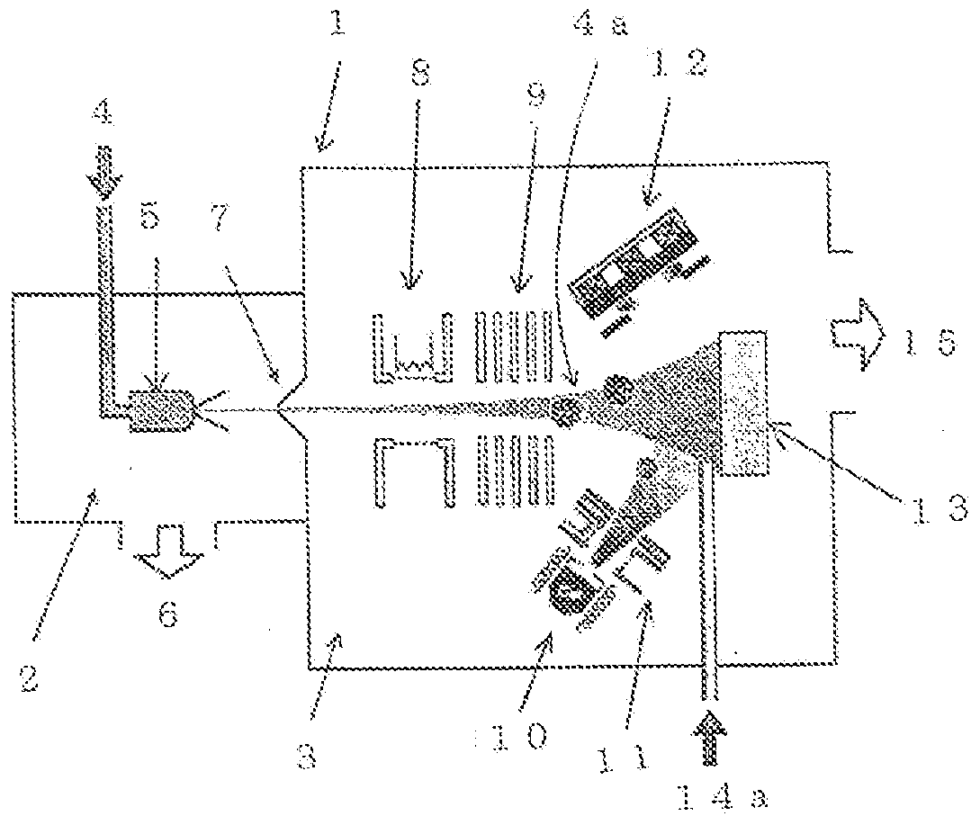
[0100] As the substrate 13 , a square silicon wafer with a size of 50 mm×50 mm was used. Mount the silicon on the figure 1 In the device shown, the 5 x 10 16 piece / cm 2 The surface of the silicon wafer is cleaned by irradiating argon cluster ions with an average number of argon atoms of 1000 accelerated at 20kV under the condition of . The number of argon atoms constituting a cluster is determined by the Time of Flight method. The argon cluster ions themselves are generated from the glass cluster generating nozzle 5 , introduced into the processing section 3 using gas cluster ions through the flow divider 7 , and are ionized by the electron collision method in the ionization section 8 to collide with the surface of the silicon wafer 13 .

[0101] After the surface of the silicon wafer is cleaned, the evaporated particles as carbonaceous materials are heated in the crucible to evaporate fullerene, and at the same time, the evaporated particles as boron materials pass through...

Embodiment 2

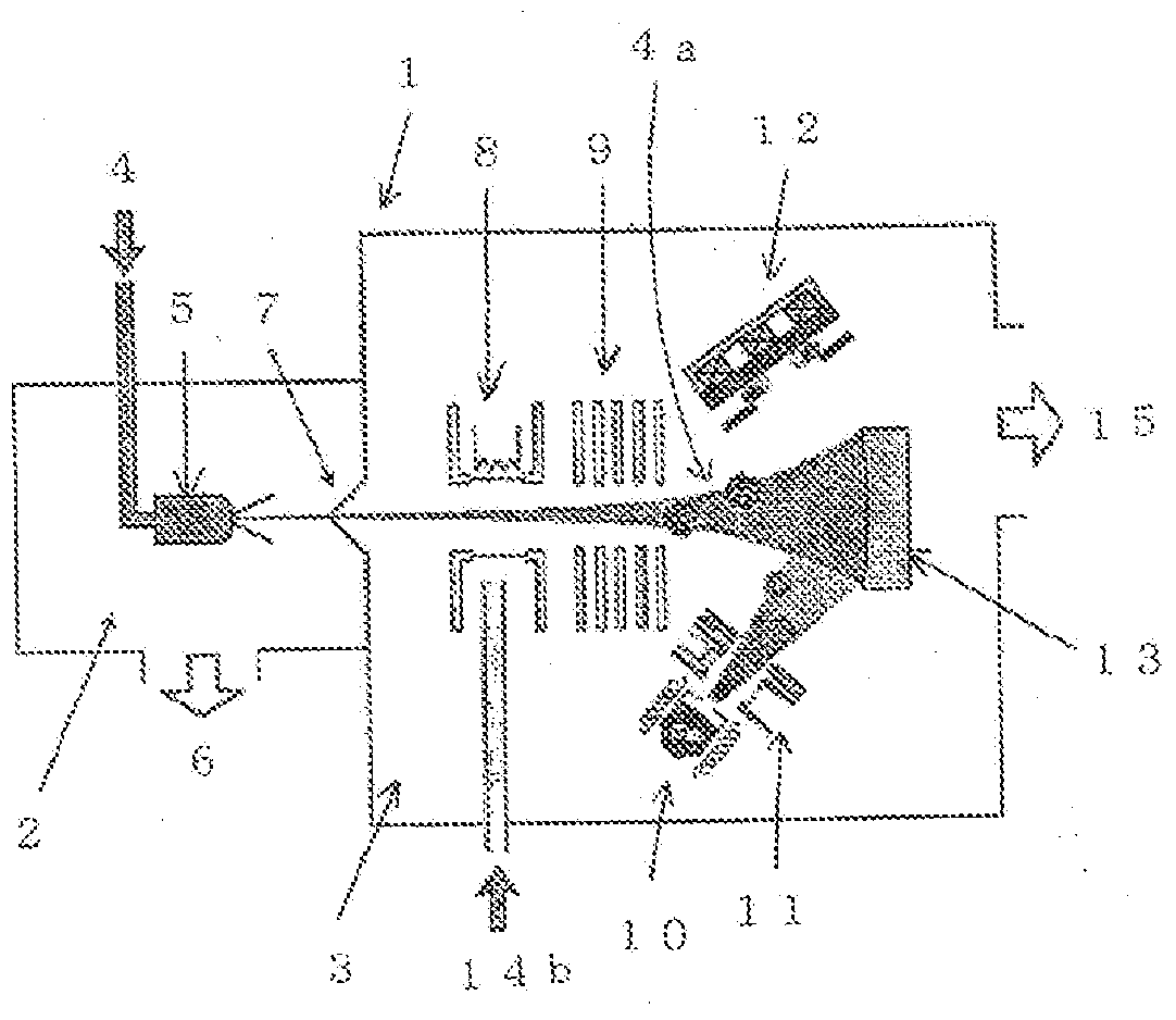
[0103] In addition to using figure 2 Except for the apparatus shown, a sample in which a boron-containing carbon film substantially free of hydrogen was formed was prepared in the same manner as in Example 1 (evaporating particles of diborane were used as the evaporating particles of boron material).

Embodiment 3

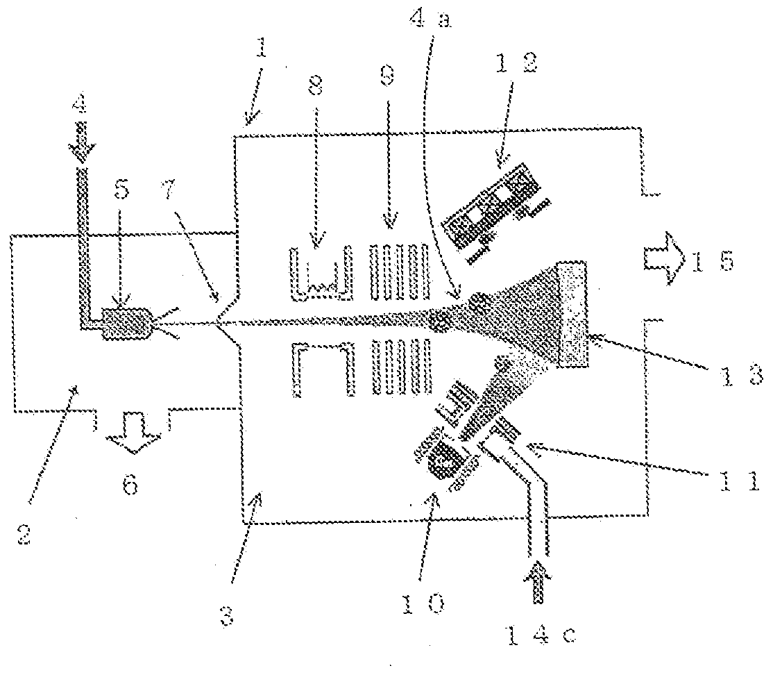
[0105] In addition to using figure 2 In the shown device, a sample having a boron-containing carbon film substantially free of hydrogen was produced in the same manner as in Example 1, except that trimethylboron was used as the boron material.


PUM

PropertyMeasurementUnit
hardnessaaaaaaaaaa
electrical resistivityaaaaaaaaaa
coating thicknessaaaaaaaaaa

Abstract

A method for forming a conductive hard carbon film in vacuum reduced pressure comprises: a step in which a gas cluster ion beam (4a) is irradiated on a substrate (13), and the substrate (13) is purified and / or flattened; a step in which an intermediate film-forming material is vaporized, the vaporization product is deposited on the surface of the substrate (13), and the gas cluster ion beam (4a) is irradiated on the intermediate film-forming material to form an intermediate film; and a step in which a carbon film-forming material containing a boron material and a carbonaceous material having substantially no hydrogen is vaporized, the vaporization product is deposited on the surface of the intermediate film, and the gas cluster ion beam (4a) is irradiated on the carbon film-forming material to form a film.

Description

technical field [0001] The present invention relates to a conductive hard carbon film and a film-forming method thereof which are applicable to various parts requiring conductivity, wear resistance, and heat resistance. In particular, it is suitable for surface treatment of probes (probes) used to measure the electrical characteristics of semiconductors and electronic component materials, surface treatment of separators provided between the anode and cathode of fuel cells, and cathode electron emission elements. Conductive hard carbon film for surface treatment etc. Background technique [0002] In recent years, conductive DLC (diamond-like carbon) has been used as a probe (probe) for measuring the electrical characteristics of semiconductors and various electronic component materials. Conventionally, as such a probe, a base material made of beryllium copper coated with gold plating has been used, but there are problems as follows. [0003] (1) Solder used for electrodes o...

Claims


Application Information

Patent Timeline
Patent Type & Authority Applications(China)
IPC IPC(8): C23C14/32C01B31/02
CPCC23C14/024C23C14/0605C23C14/22H01J37/32C01B31/02C23C16/517C23C14/221C23C14/022C23C14/3442C01B32/05G01R1/067H01B1/04Y10T428/265Y10T428/31678
Inventor 北川晃幸野村修平
Owner NOMURA PLATING CO LTD
Why Eureka
Try Eureka