Preparation methods of thyristor gate cathode junction and gate commutated thyristor with thyristor gate cathode junction

A technology of gate commutation and thyristor, which is applied in semiconductor/solid-state device manufacturing, electrical components, circuits, etc., and can solve problems such as high doping concentration

Active Publication Date: 2013-07-31
ZHUZHOU CRRC TIMES SEMICON CO LTD
View PDF6 Cites 3 Cited by
  • Summary
  • Abstract
  • Description
  • Claims
  • Application Information

AI Technical Summary

Problems solved by technology

[0010] attached by image 3 It can be seen that although the gate-cathode junction structure in the prior art and the thyristor with this structure have a large amount of electron injection from the N+ emitter region 6, due to the high doping concentration of the P+ short base region 5, a large amount of electrons are provided. The electrons recombine with the holes here to reduce the electron injection amount of the P-base region and the N-base region, which becomes a factor limiting the conductance modulation effect

Method used


Image

  • Preparation methods of thyristor gate cathode junction and gate commutated thyristor with thyristor gate cathode junction
  • Preparation methods of thyristor gate cathode junction and gate commutated thyristor with thyristor gate cathode junction
  • Preparation methods of thyristor gate cathode junction and gate commutated thyristor with thyristor gate cathode junction

Examples


Embodiment 1

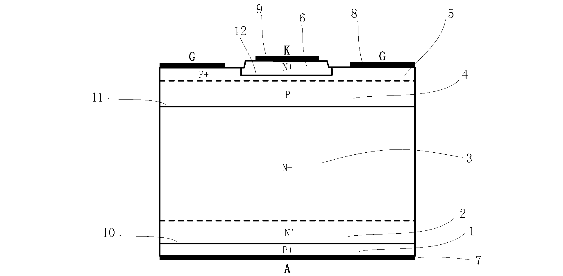
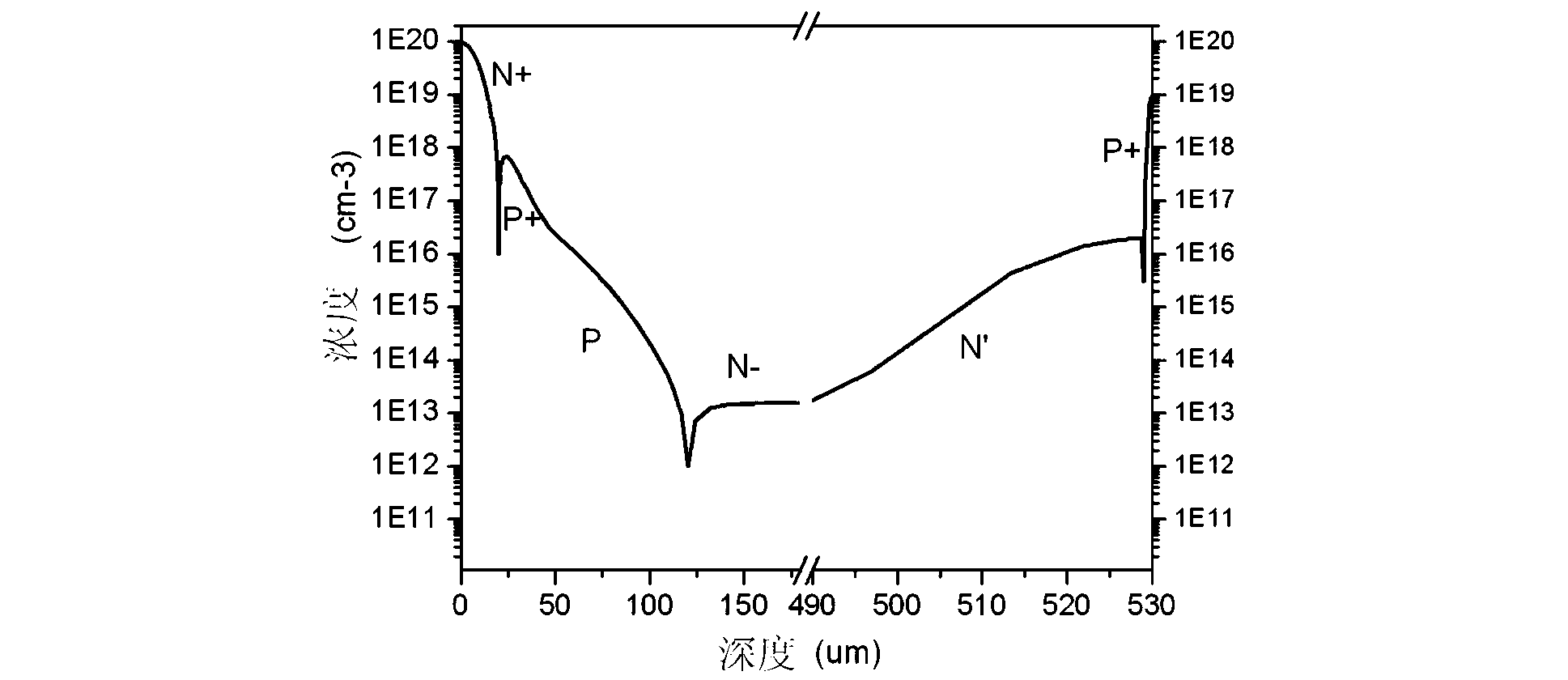
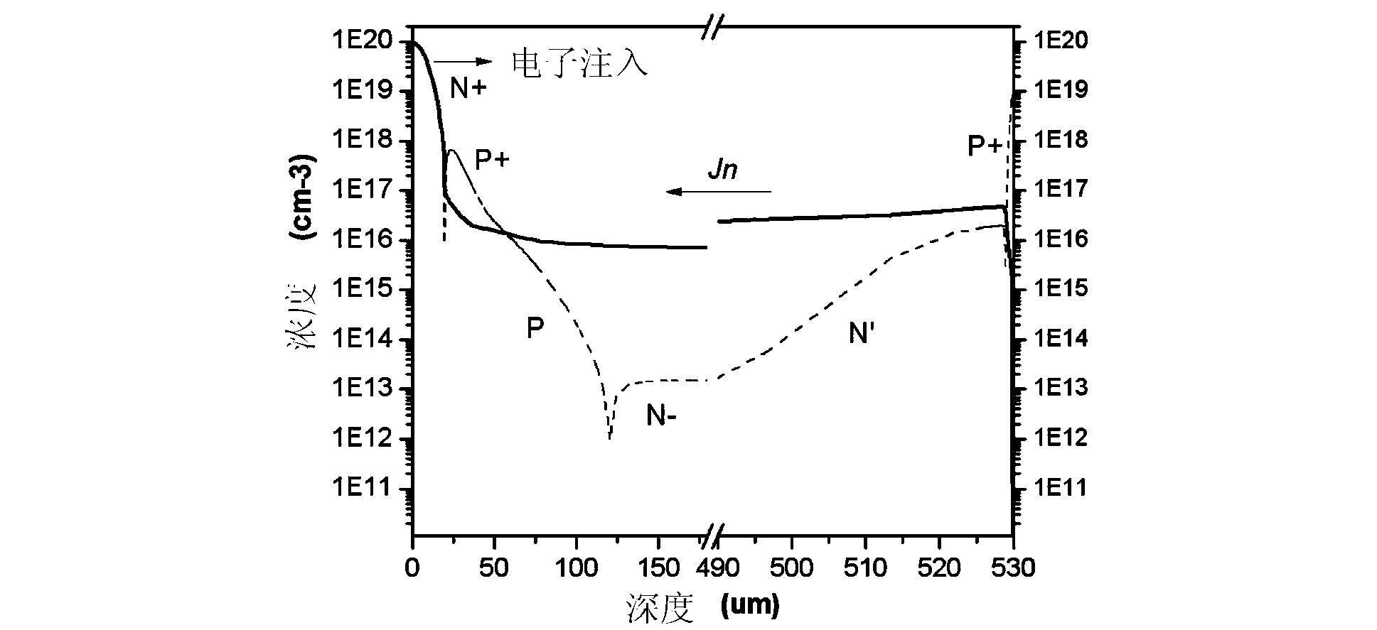
[0204] as attached Figure 43 A specific implementation method of a gate-commutated thyristor manufacturing method shown in the process of A. The gate-commutated thyristor includes more than one cell, and the manufacturing method of the gate-commutated thyristor includes more than one gate-commutated thyristor cell. The preparation method, wherein, the preparation method of a single gate commutated thyristor cell comprises the following steps:

[0205] S101: Prepare N-type substrate, as attached Figure 22 shown;

[0206] S102: Perform selective P+ diffusion treatment on the front side of the N-type substrate to form a P+ short base region 5, as shown in the attached Figure 23 As shown in the figure, the width L between the two P+ short base regions 5 is adjustable;

[0207] S103: Perform P diffusion treatment on the front side of the N-type substrate to form the P base region 4, and form the J2 junction 11 between the P base region 4 and the N-substrate 3, as shown in the...

Embodiment 2

[0218] as attached Figure 43 A specific implementation method of a gate-commutated thyristor manufacturing method shown in the process of C. The gate-commutated thyristor includes more than one cell, and the manufacturing method of the gate-commutated thyristor includes more than one gate-commutated thyristor cell. The preparation method, the preparation method of a single gate commutated thyristor cell comprises the following steps:

[0219] S301: preparing an N-type substrate;

[0220] S302: Perform P diffusion treatment on the front side of the N-type substrate to form a P base region 4, and form a J2 junction 11 between the P base region 4 and the N-substrate 3;

[0221] S303: performing selective P+ diffusion treatment on the front side of the N-type substrate to form a P+ short base region 5;

[0222] S304: performing N' diffusion treatment on the back surface of the N-type substrate to form an N' buffer layer 2;

[0223]S305: performing N+ pre-deposition treatment o...

Embodiment 3

[0234] as attached Figure 43 A specific implementation method of a gate-commutated thyristor manufacturing method shown in the process of B, the gate-commutated thyristor includes more than one cell, and the manufacturing method of the gate-commutated thyristor includes more than one gate-commutated thyristor cell The preparation method, the preparation method of a single gate commutated thyristor cell comprises the following steps:

[0235] S201: Prepare N-type substrate, as attached Figure 32 shown;

[0236] S202: Perform P' diffusion treatment on the front side of the N-type substrate, as shown in the attached Figure 33 shown;

[0237] S203: Perform selective P+ diffusion treatment on the front side of the N-type substrate to form a P+ short base region 5, as shown in the attached Figure 34 shown;

[0238] S204: Perform P diffusion treatment on the front side of the N-type substrate to form the P base region 4, and form the J2 junction 11 between the P base region ...


PUM


Abstract

The invention discloses a preparation method of a thyristor gate cathode junction and a preparation method of a gate commutated thyristor with the thyristor gate cathode junction. The preparation method of the thyristor gate cathode junction comprises the following steps of preparing an N-type substrate, conducting selective P+ diffusion treatment on the front surface of the N-type substrate to form a P+ short base region, conducting P diffusion treatment on the front surface of the N-type substrate to form a P base region, conducting N+ predeposition treatment to form an N+ layer, conducting gate etching treatment to etch off the N+ layer above a gate, conducting N+ boosting treatment on the N+ layer to form the gate cathode junction in a double-step structure, and conducting metal deposition and etching treatment to form a cathode metal electrode and a gate metal electrode respectively. According to the preparation methods of the thyristor gate cathode junction and the gate commutated thyristor with the thyristor gate cathode junction, the recombination of electrons injected into an N+ emitting region of the thyristor in the P+ short base region and the P base region can be reduced, a conductive modulation effect of the thyristor is improved, and the breakover current and breakover speed of the thyristor can be further increased.

Description

technical field [0001] The invention relates to a method for preparing a semiconductor device, in particular to a thyristor gate-cathode junction structure applied in the field of power semiconductors and a method for preparing a gate commutation thyristor with the structure. Background technique [0002] Silicon is a kind of semiconductor material. The semiconductor devices represented by silicon are all processed on the basis of the original single crystal. By doping a small amount of impurities into it, the conductivity is significantly changed, thereby forming a specific structure and doping. Miscellaneous distribution, so as to realize the function of the device. The dopants are divided into two categories: one is N-type dopants, such as phosphorus and arsenic atoms. The other type is P-type dopants, such as boron, aluminum and gallium atoms. Doping phosphorus, arsenic, and antimony can make silicon an electron-conducting type (N-type) silicon, and doping boron, alumi...

Claims


Application Information

Patent Timeline
Patent Type & Authority Applications(China)
IPC IPC(8): H01L21/332
Inventor 唐龙谷冯江华吴煜东陈勇民陈芳林
Owner ZHUZHOU CRRC TIMES SEMICON CO LTD
Why Eureka
Try Eureka