A method for improving the brightness and hardness of a nitride hard coating on the surface of a substrate
A hard coating, substrate surface technology, applied in metal material coating process, coating, ion implantation plating and other directions, can solve the problem of inability to take into account high brightness, color and high hardness, achieve good application prospects, improve Color and hardness, the effect of increasing hardness and gloss
- Summary
- Abstract
- Description
- Claims
- Application Information
AI Technical Summary
Problems solved by technology
Method used
Image
Examples
Embodiment 1
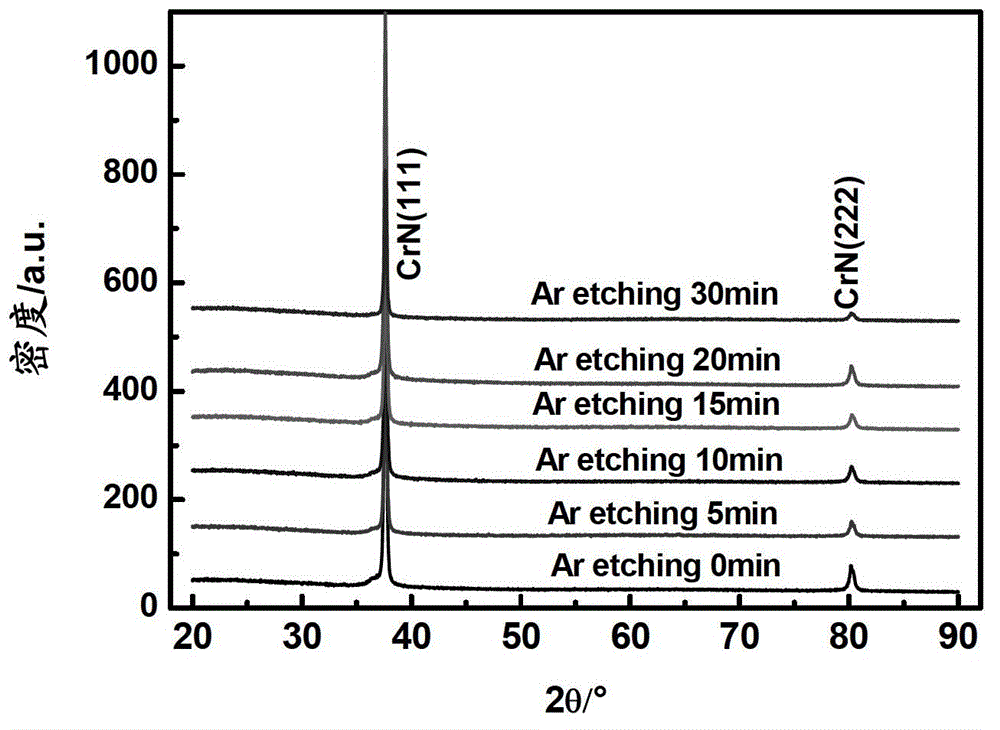
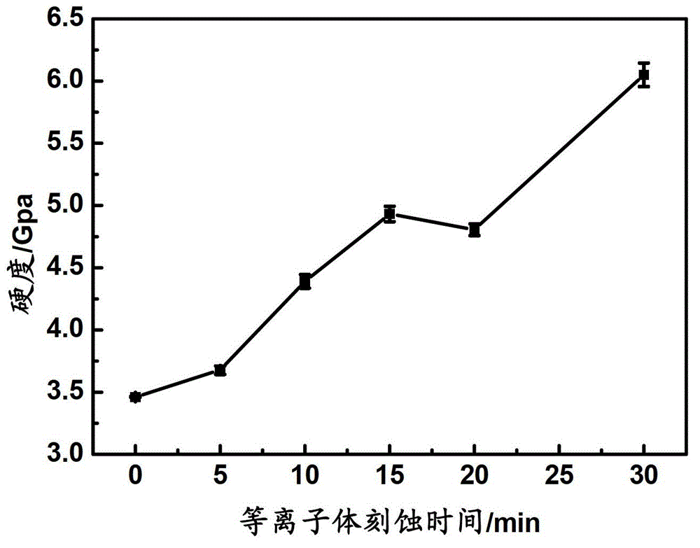
[0028] Part of the sample is taken out from the silicon wafer sample and the glass sample obtained in the above-mentioned comparative example 1 to deposit a CrN coating and carry out aftertreatment, that is, these samples are placed in the plasma equipment of argon gas, so that the plasma of argon gas is CrN coating is etched. The treatment conditions are as follows: working current 0.2A, voltage 1300V, working air pressure 2.3mtorr, treatment time is 5 minutes, 10 minutes, 15 minutes, 20 minutes, 30 minutes respectively, and there is no heating during the treatment.
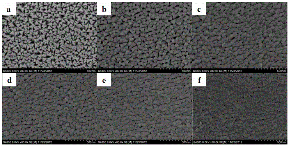
[0029] After plasma etching of argon gas for 5 minutes, 10 minutes, 15 minutes, 20 minutes and 30 minutes, the SEM surface topography of the CrN coating on the surface of the silicon wafer is as follows figure 1 Shown in (b)-(f). From figure 1 It can be seen that the CrN coating structure after argon plasma etching is denser than that of the CrN coating without argon plasma etching (a).
[0030] figure 2 It...
Embodiment 2
[0038] Part of the sample is taken out from the silicon wafer sample and the glass sample obtained in the above Comparative Example 2 for post-processing, that is, these samples are placed in the plasma equipment of argon gas, so that the plasma of argon gas is ZrN coating is etched. The treatment conditions are as follows: working current 0.3A, voltage 1500V, working air pressure 2.7mtorr, treatment time is 15 minutes respectively, no heating during treatment.
[0039] The ZrN coating on the surface of the silicon wafer obtained in Comparative Example 2 and the implementation 2 is tested as follows:
[0040] (1) Observation of SEM surface topography
[0041]The results show that, similar to the comparative results in Comparative Example 1 and Example 1, the ZrN coating after the plasma etching of argon is compared with the ZrN coating topography without the plasma etching of argon The structure is denser;
[0042] (2) XRD pattern of ZrN coating
[0043] The results show t...
Embodiment 3
[0052] The surface deposition (Cr, Al) N coated silicon wafer sample and the glass sample obtained in the above-mentioned comparative example 2 take out some samples and carry out aftertreatment, be about to these samples are placed in the plasma equipment of argon gas, make argon gas plasma to etch the ZrN coating. The treatment conditions are as follows: working current 0.1A, voltage 1500V, working air pressure 2.1mtorr, treatment time is 5 minutes respectively, no heating during treatment.
[0053] The ZrN coating on the surface of the silicon wafer obtained in Comparative Example 2 and the implementation 2 is tested as follows:
[0054] (1) Observation of SEM surface topography
[0055] The results show that, similar to the comparative results in Comparative Example 1 and Example 1, the ZrN coating after the plasma etching of argon is compared with the ZrN coating topography without the plasma etching of argon The structure is denser;
[0056] (2) XRD pattern of CrN coa...
PUM
| Property | Measurement | Unit |
|---|---|---|
| hardness | aaaaa | aaaaa |
| hardness | aaaaa | aaaaa |
| hardness | aaaaa | aaaaa |
Abstract
Description
Claims
Application Information
 - R&D
- Intellectual Property
- Life Sciences
- Materials
- Tech Scout
- Unparalleled Data Quality
- Higher Quality Content
- 60% Fewer Hallucinations
Browse by: Latest US Patents, China's latest patents, Technical Efficacy Thesaurus, Application Domain, Technology Topic, Popular Technical Reports.
© 2025 PatSnap. All rights reserved.Legal|Privacy policy|Modern Slavery Act Transparency Statement|Sitemap|About US| Contact US: help@patsnap.com


