Array multispectral optical filter and manufacturing method thereof

A production method and multi-spectral technology, applied in the direction of optical filters, etc., to achieve the effect of wide application range, reducing side lobes, and improving utilization efficiency

Active Publication Date: 2013-08-14
广东长光中科生物科技有限公司
View PDF6 Cites 42 Cited by
  • Summary
  • Abstract
  • Description
  • Claims
  • Application Information

AI Technical Summary

Problems solved by technology

[0004] In order to solve the integration problem of multi-channel array detection in the existing microfluidic chip, the present invention provides an arrayed multispectral filter suitable for microfluidic chip integration and a manufacturing method thereof

Method used


Image

  • Array multispectral optical filter and manufacturing method thereof
  • Array multispectral optical filter and manufacturing method thereof
  • Array multispectral optical filter and manufacturing method thereof

Examples


Embodiment

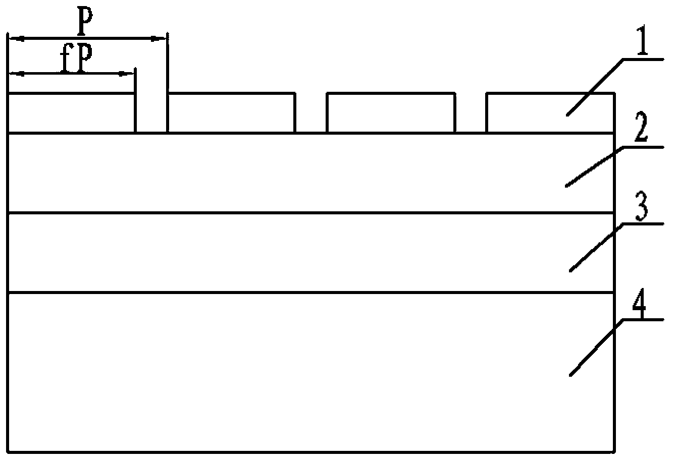
[0060] Aluminum (Al), which has high reflectivity (>90%) in the visible and infrared bands, is selected as the material of the two-dimensional metal grating layer. The buffer layer material is silicon dioxide (SiO 2 , refractive index n=1.46), the thickness is 0.1μm; the waveguide layer material is titanium dioxide (TiO 2 , refractive index n=2.5), the thickness is 0.1μm; the substrate is a quartz glass sheet (the main material is SiO 2 , Refractive index n=1.46).

[0061] Selection of various parameters:

[0062] 1. Duty cycle

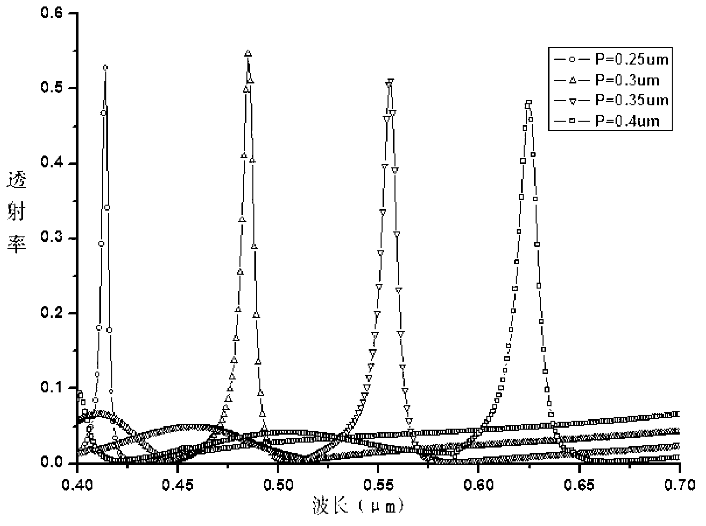
[0063] The duty cycle affects the transmittance at the peak transmittance wavelength, as shown in the attached Figure 5 shown. The figure shows that when the duty cycle f=0.7, the transmittance is as high as 85%, but at this time there will be another sub-peak near the peak wavelength, which is caused by the diffraction process of the two-dimensional metal grating, in order to avoid For the generation of this secondary peak, the duty ratio f=0....


PUM


Abstract

The invention relates to an array multispectral optical filter and a manufacturing method thereof, belongs to the field of a micro-nano optical filter and solves the problem of integration of multichannel array detection in an existing nanofluidic chip. The optical filter only comprises the following four layers of structures: a two-dimensional metal grating layer, a buffer layer, a waveguide layer and a substrate. The invention also provides the manufacturing method of the optical filter, which utilizes a guided mode resonance principle of a two-dimensional metal grating and implements selection of different wavelengths by regulating the period of the grating. By the thickness of the buffer layer, the half-wave bandwidth of the cut-off wavelength also can be regulated. By regulating a suitable duty cycle of the two-dimensional metal grating layer, side lobes can be reduced. Therefore, relative to other turnable optical filters, the array multispectral optical filter manufactured by the method disclosed by the invention has the outstanding advantages of simple structure, low side lobes, adjustability of the half-wave bandwidth, high transmittance, no relation with polarization and the like. After the optical fiber disclosed by the invention is adopted, the integration of the nanofluidic chip can be implemented.

Description

technical field [0001] The invention relates to the field of micro-nano optical filters, in particular to an array type multi-spectral optical filter and a manufacturing method thereof. Background technique [0002] Narrowband F-P thin film interference filter is a common interference filter. At present, the design of this filter is also based on the traditional F-P (Fabry-Perot) type interference filter. The traditional F-P interference filter is coated with a high reflective film on the inner surface of two parallel dielectric plates to form two reflective surfaces; a thin dielectric transparent layer is sandwiched between the two reflective surfaces; when the polychromatic light passes through, Due to interference, for light of different wavelengths, some light is strengthened by interference, and some light is destructed by interference. Therefore, after polychromatic light passes through interference, there is only light of a specific wavelength, which acts as a filter...

Claims


Application Information

Patent Timeline
Patent Type & Authority Applications(China)
IPC IPC(8): G02B5/20
Inventor 吴一辉周文超郝鹏李凯伟刘桂根刘永顺
Owner 广东长光中科生物科技有限公司
Why Eureka
Try Eureka