Assembling method of welding columns used for ceramic column grid array packaging
A technology of ceramic packaging and column grid array, which is applied in the fields of electrical components, semiconductor/solid-state device manufacturing, circuits, etc., which can solve the problems of difficult processing accuracy, high cost, and easy damage to welding posts, so as to ensure assembly accuracy and position accuracy , Easy to install, easy to use, easy to disassemble
- Summary
- Abstract
- Description
- Claims
- Application Information
AI Technical Summary
Problems solved by technology
Method used
Image
Examples
Embodiment 1
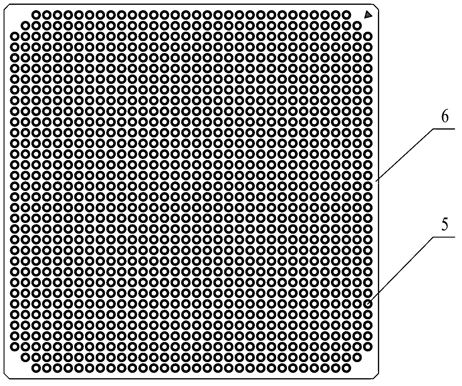
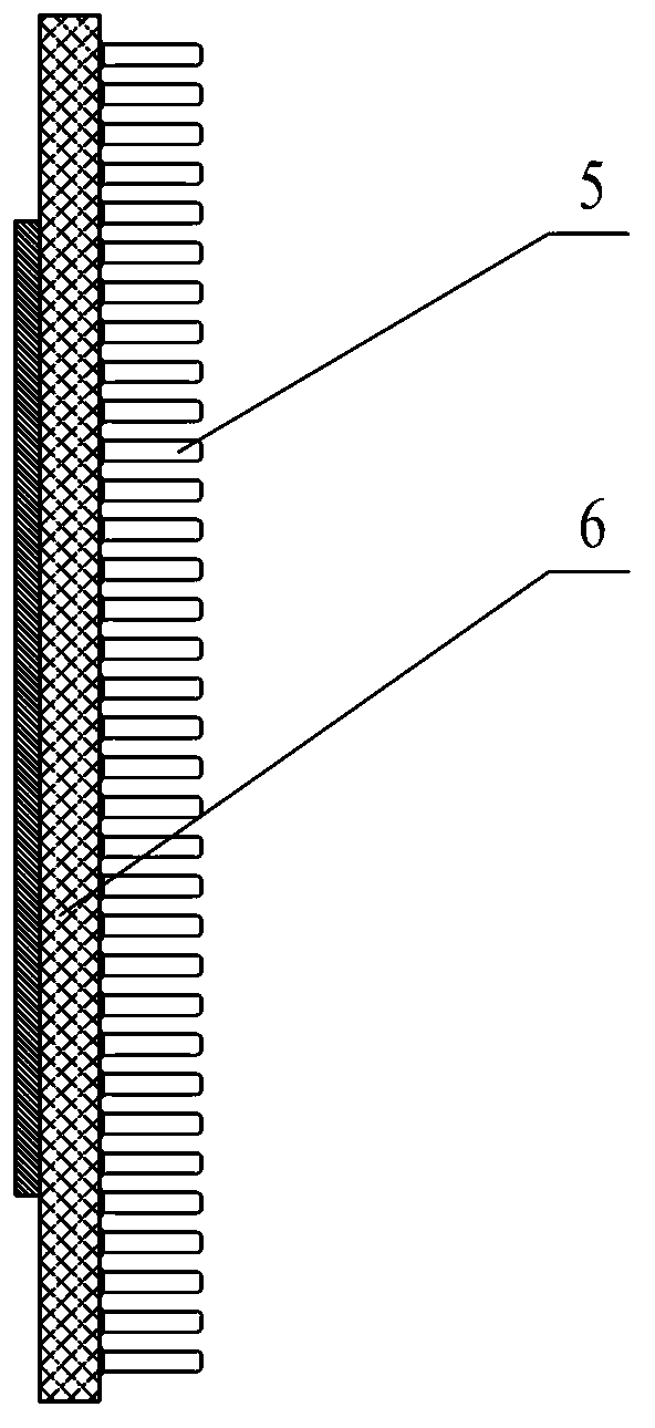
[0036] Embodiment one: if figure 1 , figure 2 As shown, a CCGA1144 packaged product with a pitch of 1.00 mm is assembled with Sn10Pb90 soldering pillars 5 with a diameter of 0.52 mm. The post welding method of this product includes the following steps:
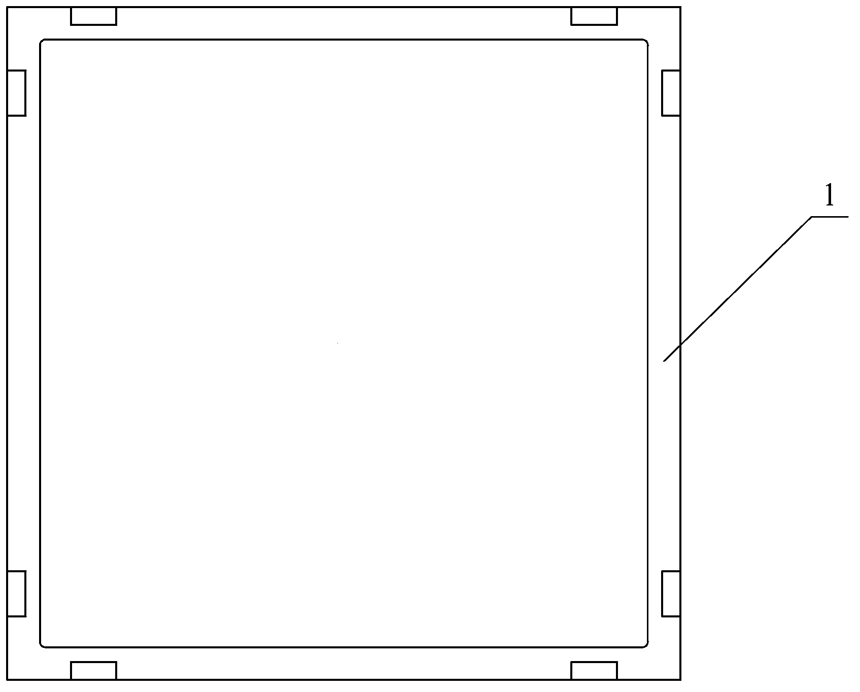
[0037] (1) if Figure 3-1 , Figure 3-2 As shown, according to the external dimensions of the CCGA1144 packaged product, the ceramic positioning frame 1 is made of Kovar alloy material, and the middle part of the ceramic positioning frame 1 is a cavity whose size and shape match the CLGA1144 circuit ceramic body 6;
[0038] (2) if Pic 4-1 , Figure 4-2 As shown, according to the external dimensions of the CCGA1144 packaged product, the carrier sheet 2 is made of Kovar alloy material with a thickness of 0.35mm, and the carrier sheet 2 is used to prevent the slipping of the welding posts 5 and ensure the coplanarity of all the welding posts 5;
[0039] (3) if Figure 5-1 , Figure 5-2As shown, according to the external...
Embodiment 2
[0045] Embodiment two: if figure 1 , figure 2 As shown, a CCGA1144 packaged product with a pitch of 1.00 mm is assembled with Sn10Pb90 soldering pillars 5 with a diameter of 0.52 mm. The post welding method of this product includes the following steps:
[0046] (1) if Figure 3-1 , Figure 3-2 As shown, according to the external dimensions of the CCGA1144 packaged product, the ceramic positioning frame 1 is made of Kovar alloy material, and the middle part of the ceramic positioning frame 1 is a cavity whose size and shape match the CLGA1144 circuit ceramic body 6;
[0047] (2) if Pic 4-1 , Figure 4-2 As shown, according to the external dimensions of the CCGA1144 packaged product, the carrier sheet 2 is made of Kovar alloy material with a thickness of 0.35mm, and the carrier sheet 2 is used to prevent the slipping of the welding posts 5 and ensure the coplanarity of all the welding posts 5;
[0048] (3) if Figure 5-1 , Figure 5-2 As shown, according to the externa...
Embodiment 3
[0054] Embodiment three: as figure 1 , figure 2 As shown, a CCGA1144 packaged product with a pitch of 1.00 mm is assembled with Sn10Pb90 soldering pillars 5 with a diameter of 0.52 mm. The post welding method of this product includes the following steps:
[0055] (1) if Figure 3-1 , Figure 3-2 As shown, according to the external dimensions of the CCGA1144 packaged product, the ceramic positioning frame 1 is made of Kovar alloy material, and the middle part of the ceramic positioning frame 1 is a cavity whose size and shape match the CLGA1144 circuit ceramic body 6;
[0056] (2) if Pic 4-1 , Figure 4-2 As shown, according to the external dimensions of the CCGA1144 packaged product, the carrier sheet 2 is made of Kovar alloy material with a thickness of 0.35mm, and the carrier sheet 2 is used to prevent the slipping of the welding posts 5 and ensure the coplanarity of all the welding posts 5;
[0057] (3) if Figure 5-1 , Figure 5-2 As shown, according to the exter...
PUM
| Property | Measurement | Unit |
|---|---|---|
| Thickness | aaaaa | aaaaa |
| Thickness | aaaaa | aaaaa |
Abstract
Description
Claims
Application Information


