Reverse block (RB)-insulated gate bipolar transistor (IGBT) device provided with double-faced field stop with buried layers

A field stop layer and field stop technology, applied in semiconductor devices, electrical components, circuits, etc., can solve the problems of large turn-off power consumption, high turn-on voltage drop of devices, and thick drift region, so as to improve forward and reverse endurance The effect of reducing the voltage level, reducing the forward conduction voltage drop, and optimizing the carrier concentration distribution

Inactive Publication Date: 2013-08-21
UNIV OF ELECTRONIC SCI & TECH OF CHINA +1
View PDF6 Cites 19 Cited by
  • Summary
  • Abstract
  • Description
  • Claims
  • Application Information

AI Technical Summary

Problems solved by technology

[0004] In the conventional RB-IGBT structure, due to the NPT structure of the cells, the drift region is thicker, resulti

Method used


Image

  • Reverse block (RB)-insulated gate bipolar transistor (IGBT) device provided with double-faced field stop with buried layers
  • Reverse block (RB)-insulated gate bipolar transistor (IGBT) device provided with double-faced field stop with buried layers
  • Reverse block (RB)-insulated gate bipolar transistor (IGBT) device provided with double-faced field stop with buried layers

Examples


Embodiment Construction

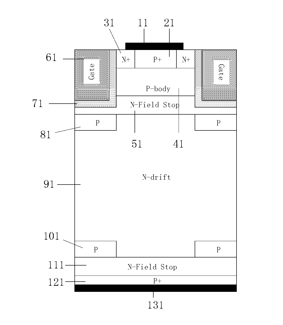
[0021] An RB-IGBT device with a double-sided field stop band buried layer, such as image 3 shown, including P + collector area 121, located at P + The metal anode 131 on the back of the collector region 121 is located at P + N on the front side of the collector region 121 — Drift Zone 91, at N — The P-type base region 41 above the drift region 91, the surface of the P-type base region 41 has P + Ohmic contact area 21 and N + source region 31, with P + Ohmic contact area 21 and N + The metal cathode electrode 11 that is in contact with the surface of the source region 31; also includes a polysilicon gate electrode 61, and the polysilicon gate electrode 61 is connected to the P-type base region 41 and the N + There is a gate oxide layer 71 between the source regions 31 . The P-type base region 41 and N — There is also a front N-type field stop layer 51 between the drift regions 91, the P+ collector region 121 with N — There is also a rear N-type field stop layer 111 b...


PUM


Abstract

The invention discloses a reverse block (RB)-insulated gate bipolar transistor (IGBT) device provided with double-faced field stop with buried layers, and belongs to the technical field of power semiconductor devices. On the basis of a common RB-IGBT structure, an N-type FS ( Field Stop) layer is introduced between a P-type base region and an N-type drift region, an N-type FS ( Field Stop) layer is introduced between the N-type drift region and a P+ collector region, and meanwhile, P-type buried layers are introduced below a front field stop layer and above a back field stop layer. Under the condition that a device voltage withstanding requirement is met, the electric fields of the device are distributed in a trapezoid mode replacing a triangular mode by a manner that the thickness of the device is reduced. Carrier concentration distribution in the drift region is optimized, so that conductivity modulation in the device is enhanced, and forward direction breakover drop voltage and turn-off loss of the device are reduced.

Description

technical field [0001] The invention belongs to the technical field of power semiconductor devices, and in particular relates to a reverse-resistance insulated gate bipolar transistor with a double-sided field stop band buried layer. Background technique [0002] Insulated Gate Bipolar Transistor (Insulated Gate Bipolar Transistor) is the most representative device in current medium and high power power systems. It not only has the advantages of easy driving of MOSFET, simple control and high switching frequency, but also the advantage of conduction voltage drop of power transistor. In view of these advantages of IGBT, it is widely used in civil, industrial and national defense fields. [0003] In a power AC-AC matrix system, each line needs to have bidirectional blocking capability. Because the traditional IGBT chip has no junction terminal structure in the back area, it cannot withstand the reverse withstand voltage, so it must be used in series with diodes, such as fig...

Claims


Application Information

Patent Timeline
IPC IPC(8): H01L29/739H01L29/06
Inventor 李泽宏杨文韬宋洵奕陈钱单亚东张金平任敏
Owner UNIV OF ELECTRONIC SCI & TECH OF CHINA
Why Eureka
Try Eureka