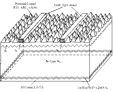
Method for preparing N-type substrate microcrystalline silicon hetero-junction cell based on SE selective emitter junction

A heterojunction cell, selective technology, applied in circuits, electrical components, climate sustainability, etc., can solve the problems of difficult passivation of silicon wafers, low photoelectric conversion rate, etc., to improve photoelectric conversion rate and low cost , easily compatible effects

Inactive Publication Date: 2013-08-21
GCL SYST INTEGRATION TECH
View PDF6 Cites 6 Cited by
  • Summary
  • Abstract
  • Description
  • Claims
  • Application Information

AI Technical Summary

Problems solved by technology

[0003] The purpose of the present invention is to overcome the problems of low photoelectric conversion rate and difficult passivation treatment of silicon wafers in the prior art, and proposes a method for preparing an N-type substrate microcrystalline silicon heterojunction cell based on an SE selective emission junction. On the surface of the silicon wafer, the above problems can be solved

Method used


Image

  • Method for preparing N-type substrate microcrystalline silicon hetero-junction cell based on SE selective emitter junction

Examples


Embodiment 1

[0023] Example 1: (1) Cleaning the silicon wafer substrate for texturing: first use NaOH solution to remove the damaged layer of the silicon wafer substrate; then use KOH solution, isopropyl alcohol IPA and texturing additives to etch the textured surface; After soaking in HCL solution, rinse with deionized water and dry.

[0024] (2) Print phosphor ink on the front side of the silicon wafer through a screen and dry it: on the special SE phosphor ink screen, use screen printing technology to transfer the phosphor ink to the N-type silicon wafer substrate, and dry it for use .

[0025] (3) Then diffuse the silicon wafer to form a selective emission junction N+ diffusion layer on the front side of the silicon wafer: put the silicon wafer substrate into the diffusion furnace, and perform one-time diffusion with phosphorus oxychloride as the liquid diffusion source. The temperature of the diffusion furnace is controlled at 820° C., and the diffusion time is 25 minutes, so that th...

Embodiment 2

[0032] Example 2: (1) First use NaOH solution to remove the damaged layer of the silicon wafer substrate; then use KOH solution, isopropanol IPA and texturing additives to etch the textured surface, and finally soak in HCL solution, then use deionized water Rinse, dry.

[0033] (2) On the special SE phosphor ink screen, use screen printing technology to transfer the phosphor ink to the N-type silicon wafer substrate, and dry it for use.

[0034] (3) Put the silicon wafer substrate into the diffusion furnace, and perform one-time diffusion with phosphorus oxychloride as the liquid diffusion source. The temperature of the diffusion furnace is controlled at 850° C., and the diffusion time is 30 minutes, so that the square resistance of the selective diffusion area is controlled at 75 ohm / square, and the surface resistance of the non-reexpanded area is controlled at 35 ohm / square.

[0035] (4) Secondary cleaning of silicon wafers.

[0036] (5) The N+ front of the battery is etch...

Embodiment 3

[0041] Example 3: (1) First use NaOH solution to remove the damaged layer of the silicon wafer substrate; then use KOH solution, isopropanol IPA and texturing additives to etch the textured surface, and finally soak in HCL solution, then use deionized water Rinse, dry.

[0042] (2) On the special SE phosphor ink screen, use screen printing technology to transfer the phosphor ink to the N-type silicon wafer substrate, and dry it for use.

[0043] (3) Put the silicon wafer substrate into the diffusion furnace, and perform one-time diffusion with phosphorus oxychloride as the liquid diffusion source. The temperature of the diffusion furnace is controlled at 860° C., and the diffusion time is 35 minutes, so that the square resistance of the selective diffusion area is controlled at 80 ohm / square, and the surface resistance of the non-reexpanded area is controlled at 40 ohm / square.

[0044] (4) Secondary cleaning of silicon wafers.

[0045] (5) The N+ front of the battery is etch...


PUM


Abstract

The invention relates to a method for preparing an N-type substrate microcrystalline silicon hetero-junction cell based on an SE selective emitter junction. The method for preparing the N-type substrate microcrystalline silicon hetero-junction cell based on the SE selective emitter junction is characterized in that an N-type silicon wafer serves as a cell substrate, and the method comprises the following steps that the wafer substrate is washed and a texture surface is made, phosphorus ink is printed on the front face of the silicon wafer through a silk screen and drying is carried out, the silicon wafer is diffused and an N+ diffusing layer of the selective emitter junction is formed on the front face of the silicon wafer, secondary washing is carried out on the silicon wafer, an a-SiNx layer is deposited on the N+ diffusing layer, an amorphous silicon/microcrystalline laminating structure is deposited on the back face of the cell, an electrode of the front face of the silicon wafer is printed through the silk screen, and an electrode of the back face of the silicon wafer is sputtered and evaporated. The method for preparing the N-type substrate microcrystalline silicon hetero-junction cell based on the SE selective emitter junction has the advantages that a processing technology is simple and rapid, cost is low, the method can be easily compatible with a cell technology of an existing process, an inactivation effect is excellent, a photoelectric conversion rate is greatly improved, and using performance of the cell is improved.

Description

technical field [0001] The invention relates to a method for manufacturing a microcrystalline silicon heterojunction battery, in particular to a method for preparing an N-type substrate microcrystalline silicon heterojunction battery based on an SE selective emission junction. Background technique [0002] The efficiency improvement of high-efficiency crystalline silicon cells based on traditional processes has gradually come to an end, and the development of high-efficiency, low-cost cell technologies that are easily compatible with existing mainstream processes is becoming more and more urgent. Various structural types of selective emitter junction SE battery solutions have also emerged, but the industrialized SE technology route has limited improvement in battery performance. In the current industrial battery structure with a battery efficiency of more than 20%, SANYO's HIT battery is famous for its high open circuit voltage and simple process. The present invention comb...

Claims


Application Information

Patent Timeline
Patent Type & Authority Applications(China)
IPC IPC(8): H01L31/18
CPCY02P70/50
Inventor 高华汪建强张闻斌李杏兵杨达伟
Owner GCL SYST INTEGRATION TECH
Why Eureka
Try Eureka