Thin-film encapsulation structure of top light-emitting OLED device and preparing method thereof
A thin-film packaging and top-emitting technology, which is applied in semiconductor/solid-state device manufacturing, electric solid-state devices, semiconductor devices, etc., can solve the problem of luminous attenuation device efficiency and life attenuation, higher than the tolerance range of OLED devices, organic materials or metal electrode damage and other problems, to achieve the effects of simplifying the production process, facilitating popularization and use, and convenient operation
- Summary
- Abstract
- Description
- Claims
- Application Information
AI Technical Summary
Problems solved by technology
Method used
Image

Examples
Embodiment 1
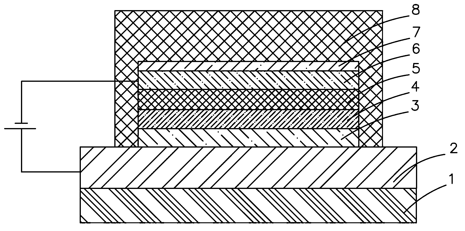
[0029] The thin-film encapsulation structure of the top-emitting OLED device in this embodiment, such as figure 1 Said, including the substrate 1 and the reflective anode 2, the hole transport layer 3, the light emitting layer 4, the electron transport layer 5, the translucent cathode 6 and the thin film encapsulation layer 8 stacked on the substrate 1 in sequence, and also includes the encapsulation buffer layer 7, The encapsulation buffer layer 7 is disposed between the translucent cathode 6 and the thin film encapsulation layer 8 .
[0030] Wherein, the encapsulation buffer layer 7 is a red-emitting fluorescent material with a thickness of 1 nm, such as coumarin, aromatic compounds and their derivatives.
[0031] The preparation method of the thin-film encapsulation structure of the top-emitting OLED device described in this embodiment comprises the following steps:
[0032] Step 1: The reflective anode 2, the hole transport layer 3, the light emitting layer 4, the electro...
Embodiment 2
[0038] The thin film encapsulation structure of the top-emitting OLED device in the present embodiment, its structure is the same as embodiment 1, as figure 1 shown.
[0039] The encapsulation buffer layer 7 of the thin-film encapsulation structure of the top-emitting OLED device is a fluorescent light-emitting material with a thickness of 3 nm and emitting green light, such as coumarin derivatives, quinacridone and its derivatives, polycyclic aromatic hydrocarbons, etc. Compounds and their derivatives, green fluorescent dopants of 1H-pyrazolo[3,4-b]quinoxaline.
[0040] The preparation method of the thin-film encapsulation structure of the top-emitting OLED device described in this embodiment comprises the following steps:
[0041] Step 1: The reflective anode 2, the hole transport layer 3, the light emitting layer 4, the electron transport layer 5, and the translucent cathode 6 are sequentially prepared on the substrate 1 by thermal evaporation method;
[0042] Step 2: Pre...
Embodiment 3
[0047] The thin-film encapsulation structure of the top-emitting OLED device in the present embodiment, its structure is the same as embodiment 1, as figure 1 shown.
[0048] The encapsulation buffer layer 7 of the thin-film encapsulation structure of the top-emitting OLED device is a fluorescent light-emitting material with a thickness of 6 nm and blue light, such as TBP, TPP, DSA, DSA-Ph, BD-1, BD-2, BD-3 .
[0049] The preparation method of the thin-film encapsulation structure of the top-emitting OLED device comprises the following steps:
[0050] Step 1: The reflective anode 2, the hole transport layer 3, the light emitting layer 4, the electron transport layer 5, and the translucent cathode 6 are sequentially prepared on the substrate 1 by thermal evaporation;
[0051] Step 2: Prepare the encapsulation buffer layer 7 on the plated translucent cathode 6 by thermal evaporation;
[0052] In step 3, a polymer film encapsulation layer is prepared on the encapsulation buffe...
PUM
| Property | Measurement | Unit |
|---|---|---|
| Thickness | aaaaa | aaaaa |
| Thickness | aaaaa | aaaaa |
Abstract
Description
Claims
Application Information
 - R&D
- Intellectual Property
- Life Sciences
- Materials
- Tech Scout
- Unparalleled Data Quality
- Higher Quality Content
- 60% Fewer Hallucinations
Browse by: Latest US Patents, China's latest patents, Technical Efficacy Thesaurus, Application Domain, Technology Topic, Popular Technical Reports.
© 2025 PatSnap. All rights reserved.Legal|Privacy policy|Modern Slavery Act Transparency Statement|Sitemap|About US| Contact US: help@patsnap.com