

Method for improving field emission performance of material
A field emission and performance technology, which is used in the manufacture of discharge tubes/lamps, laser welding equipment, electrical components, etc. The effect of electron emission performance, low cost and simple operation
- Summary
- Abstract
- Description
- Claims
- Application Information
AI Technical Summary
Problems solved by technology
Method used
Image

Examples
Embodiment 1
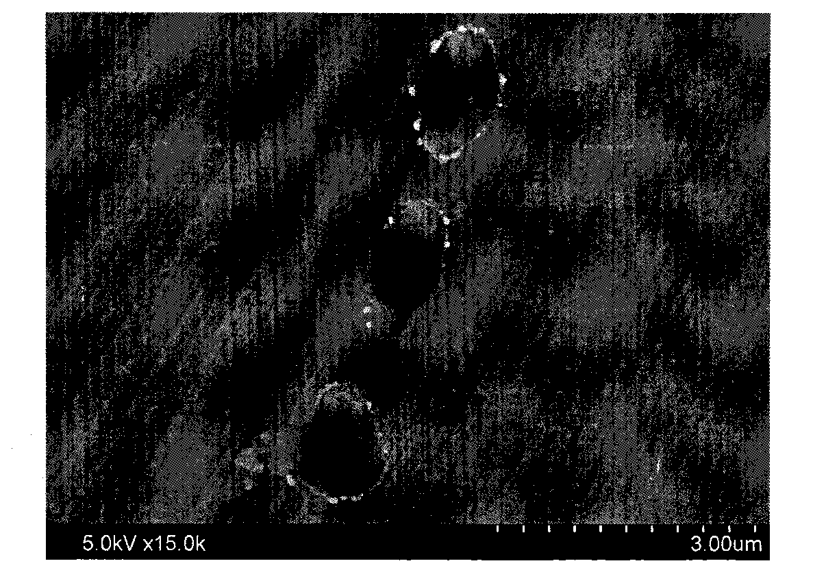
[0015] A method for improving the field emission performance of materials, the specific steps are: make a dot matrix image in the corresponding computer software of the laser marking machine, and set the power density of the laser marking machine to 2W / cm 2 , using a carbon dioxide laser with a marking speed of 300 mm / s, using the laser marking machine to perform laser treatment on the surface of the carbon film material of the field emission cathode material for 9 seconds by using a scanning processing method to form a regular micro-nano structure, such as figure 1 So not.
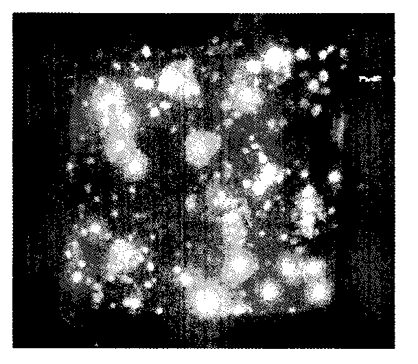
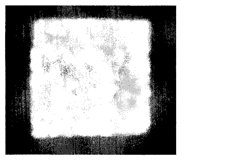
[0016] The carbon thin film material that has not been treated by the above method and the carbon thin film material that have been treated by the method of topping are tested for field emission performance. With a field emission instrument, the current change is observed by applying a voltage after vacuuming. The field emission vacuum degree is 2×10 -5 Pa, figure 2 It is the field emission rendering of...
PUM
 Abstract
Description
Claims
Application Information