Composite field electronic emitting material and preparation method and use thereof

An electron emitter and composite field technology, which is applied in the manufacture of electrode systems, discharge tube electron guns, discharge tubes/lamps, etc., can solve the problems of high cost and high equipment requirements, and achieve the effect of improving the performance of field electron emission

Inactive Publication Date: 2009-09-09
WUHAN UNIV
View PDF2 Cites 0 Cited by
  • Summary
  • Abstract
  • Description
  • Claims
  • Application Information

AI Technical Summary

Problems solved by technology

3. Other methods such as laser melting, arc discharge and other equipment require high equipment and are expensive
The growth of one-dimensional carbon nanomaterials on low-dimensional nanostructured oxides as a field emission cathode has not been reported so far

Method used


Image

  • Composite field electronic emitting material and preparation method and use thereof
  • Composite field electronic emitting material and preparation method and use thereof
  • Composite field electronic emitting material and preparation method and use thereof

Examples


Embodiment 1

[0025] 1. Use semiconductor standard cleaning technology for silicon wafers (such as: Yan Zhirui, Development Direction of Semiconductor Silicon Wafer Cleaning Technology, Special Equipment for Electronic Industry, 2003, September, p23-26), to clean single-sided polished silicon wafers. Using a pulsed laser deposition system (such as Xin Chen, Wenjie Guan, Guojia Fang, Xingzhong Zhao, Influence of substrate temperature and post-treatment on properties of ZnO: Althin films prepared by pulsed laser deposition, Appl.Surf.Sci., 2005, 252 (5 ): 1561-1567.), deposit a zinc oxide film with a thickness of 100-500nm on the polished surface of the cleaned silicon wafer.

[0026] 2. Put 0.1-1 gram of zinc oxide and graphite powder mixture (molar ratio 1:1) at the bottom of the sealed end of the quartz tube sealed at one end, and put the silicon wafer deposited with the zinc oxide film into the quartz tube sealed at one end , and 5-10cm away from the bottom of the sealed end.

[0027] 3....

Embodiment 2

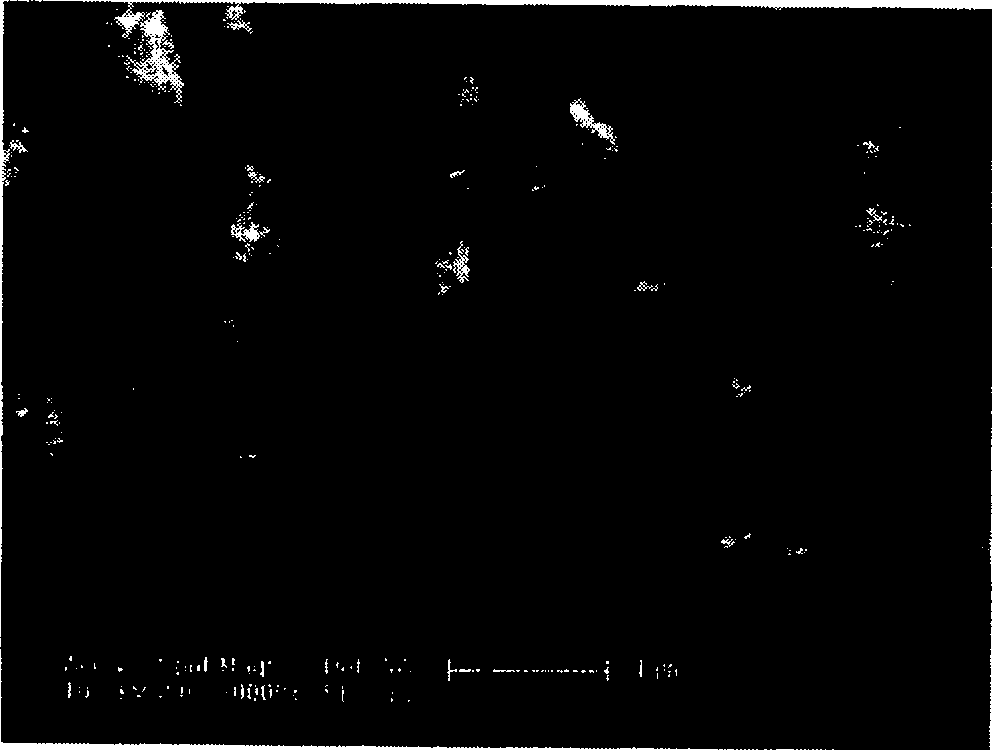
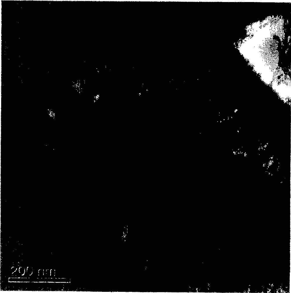
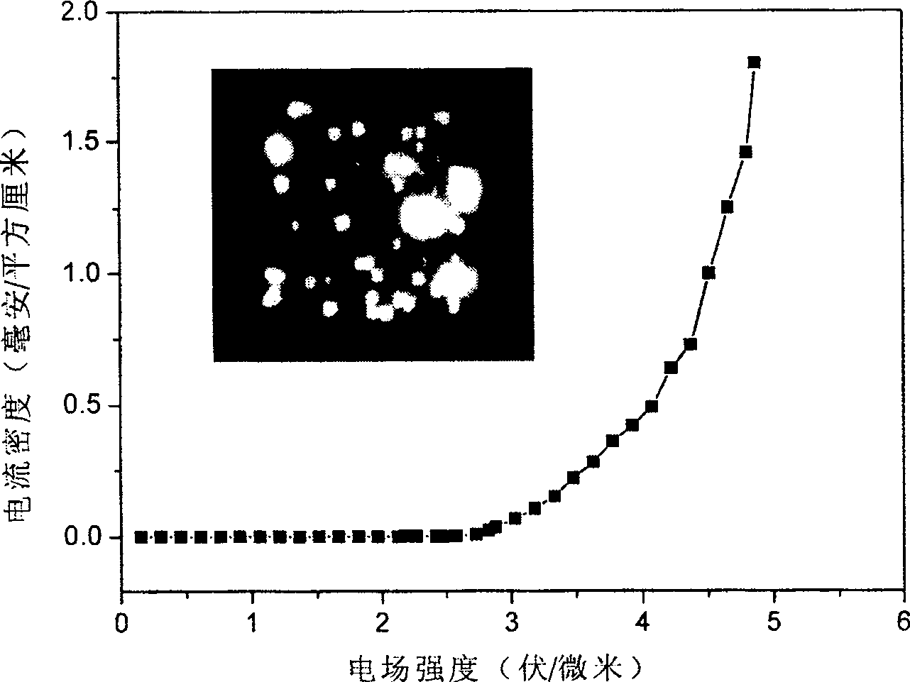
[0032] Embodiment 2: use magnetic on the obtained indium oxide nanowires (preparation method is the same as reference Qing Wan, Eric N Dattoli, Wayne Y.Fung, et al., Nano Letters, 2006, 6 (12): 2909-2915) Metal iron with a thickness of about 5 nanometers was plated by controlled sputtering. Burn in liquefied petroleum gas flame for 5 minutes. Carbon nanotubes and carbon nanofibers can be grown on indium oxide nanowires to obtain a one-dimensional carbon nanomaterial cathode emitter based on indium oxide nanowires. (other subsequent processing is the same as example 1). The measured electric field intensity and current density characteristic curve of the indium oxide nanowire array / one-dimensional carbon nanomaterial composite cathode emitter is as follows: Figure 4 .

Embodiment 3

[0033] Embodiment 3: 1. Use magnetron sputtering to plate a gold film with a thickness of about 10 nanometers on the polished surface of a silicon wafer as a catalyst. 2. Put the silicon chip coated with gold film together with the powder mixture of tin dioxide and graphite (molar ratio 1:1) into the tube atmosphere furnace, place the silicon chip under the air flow, about 5cm away from the powder mixture, 900-1100 degrees for 30-60 minutes, argon gas flow 50-200sccm. Then it can be taken out with the furnace cooling down to normal temperature, and the tin dioxide nanobelt can be obtained on the silicon wafer. 3. Plating 50 nm of cobalt (Co) on the tin dioxide nanoribbons. Put the nickel-plated surface of the substrate down, and burn it in the middle of the burning acetylene flame for 10 minutes. Carbon nanotubes and carbon nanofibers can grow on the tin oxide nanobelts, and one-dimensional carbon nanometers based on tin oxide nanobelts can be obtained. Material Cathode Emit...


PUM


Abstract

The invention relates to a compound field electron emitter, which comprises a conductive substrate, and uses oxide nanowires, nanobelts or nanorods attached to the conductive substrate as a substrate, and one-dimensional carbon nanomaterials grow on the substrate. The preparation method of the composite field electron emitter is as follows: growing oxide nanowires, nanobelts or nanorods on a conductive substrate, plating a transition metal catalyst on the surface of the oxide nanowires, nanobelts or nanorods, and then Burn for 1-30 minutes to form a composite field electron emitter of one-dimensional carbon nanomaterials with oxide nanowires, nanobelts or nanorods as the matrix. The preparation process of the invention is simple and the cost is low, and the prepared composite field electron emission material can be used as an emission cathode in a field emission display, a luminous light source, an X-ray electron source, a mass spectrometer electron source and other occasions requiring electron sources.

Description

technical field [0001] The present invention relates to nano-oxide and one-dimensional carbon nano-material composite field electron emission low-dimensional nano-material and its preparation method and application, especially relates to a kind of carbon nano-material synthesized on low-dimensional oxide nano-material and used as field emission The cathode belongs to the field of nanomaterial preparation and application, and also belongs to the field of vacuum microelectronics. Background technique [0002] Due to its unique structure and physical properties, one-dimensional nanomaterials not only provide valuable research objects for basic physics research, but also herald huge market application prospects, which will surely bring revolutionary changes to traditional materials and microelectronics. . One-dimensional nanomaterials such as nanowires and nanotubes have large aspect ratios and extremely small tip radii, which can be used as excellent field emission sources, an...

Claims


Application Information

Patent Timeline
Patent Type & Authority Patents(China)
IPC IPC(8): H01J1/304H01J3/02H01J9/02B82B1/00B82B3/00
Inventor 方国家李春袁龙炎刘逆霜
Owner WUHAN UNIV
Why Eureka
Try Eureka