Single-chip bridge-type magnetic field sensor

一种磁场传感器、单芯片的技术,应用在磁传感器领域,能够解决降低传感器线性度、温度补偿功能降低、磁场动态范围减小等问题,达到良好线性度和高灵敏度、改善温度补偿性能、增大动态范围的效果

Active Publication Date: 2013-08-28
MULTIDIMENSION TECH CO LTD
View PDF11 Cites 64 Cited by
  • Summary
  • Abstract
  • Description
  • Claims
  • Application Information

AI Technical Summary

Problems solved by technology

However, this method will lead to a decrease in the dynamic range of the magnetic field that the sensor responds to, resulting in a decrease in the sensitivity of the sensor
[0006] (3) Reference bridge sensors using magnetic shielding or flux concentrators. Due to the long distance between the reference arm and the sensing arm, the current sensor is large in size, high in cost, and difficult to control the output offset
The silicon substrate 1 has a large length along the sensing axis direction 100, and the sensing element 3 and the reference element 4 are far apart, that is, the distance between the sensing arm and the reference arm is relatively large, and there is only one The gap is 5, which will cause a waste of space on the chip and make the size of the chip relatively large. The size of the chip designed in this way is about 2mm X 0.5mm
Moreover, due to the relatively large distance between the sensing arm and the reference arm, it will make the bridge difficult to balance, and will cause the temperature on the two arms to be different, resulting in a decrease in its temperature compensation function
In addition, due to the use of the square shielding structure 2, the sensor will more easily reach the saturation state of the magnetic field, and a non-uniform saturated magnetic field will start to be generated near the center of the shielding structure 2, and hysteresis will be generated near the gap 5, thereby Reduced sensor linearity

Method used


Image

  • Single-chip bridge-type magnetic field sensor
  • Single-chip bridge-type magnetic field sensor
  • Single-chip bridge-type magnetic field sensor

Examples


Embodiment 1

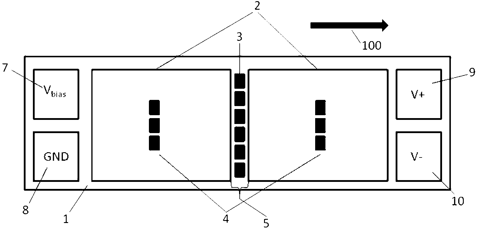
[0072] figure 2 It is a structural schematic diagram of the single-chip full-bridge magnetic field sensor of the present invention. The sensor includes a substrate 1, a Wheatstone full bridge deposited on the substrate 1, eight shielding structures 42 and four pads 7-10. The Wheatstone full bridge includes a first bridge arm and a second bridge arm electrically connected to each other, the first bridge arm includes a reference arm R1 and a sensing arm S1, the second bridge arm includes a reference arm R2 and a sensing arm S2, and the reference arm R1 R2 and R2 respectively include 3 rows of first reference element strings and 3 rows of second reference element strings, sensing arms S1 and S2 respectively include 3 rows of first sensing element strings and 3 rows of second sensing element strings, each reference element string and each Each sensing element string is composed of one or more identical magnetoresistive sensing elements electrically connected. The reference arm R...

Embodiment 2

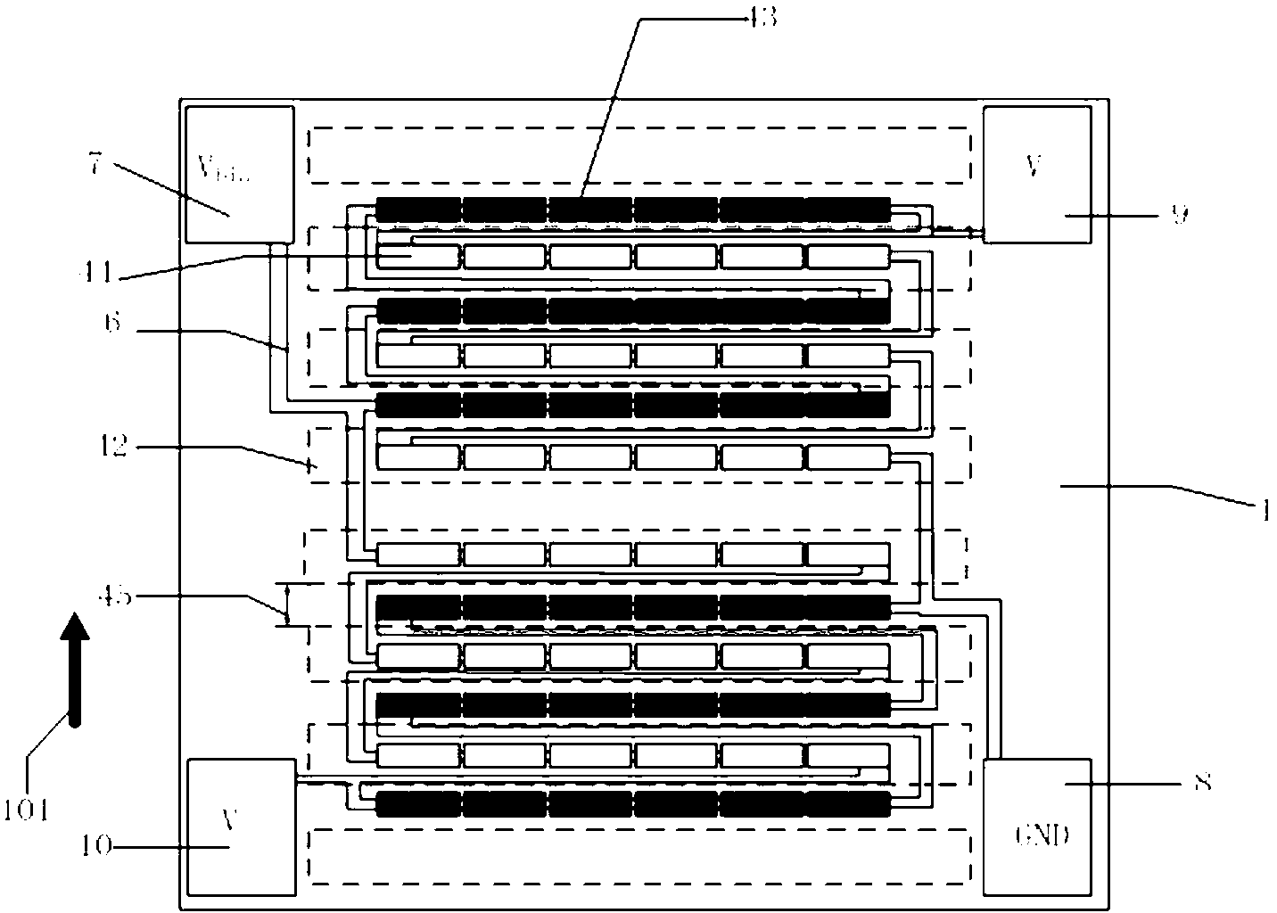
[0085] Figure 12 It is a structural schematic diagram of the single-chip half-bridge magnetic field sensor of the present invention. The sensor includes a substrate 1, a Wheatstone half bridge deposited on the substrate 1, six shielding structures 42 and three pads 7-9. The Wheatstone half-bridge includes a reference arm R1 and a sensing arm S1, each of which includes 3 rows of reference element strings 44 and 3 rows of sensing element strings 43, each reference element string 44 and each sensing element Each of the strings 43 is formed by electrically connecting one or more identical magnetoresistive sensing elements, 6 magnetoresistive sensing elements are shown in the figure. The reference element strings 44 and the sensing element strings 43 are arranged at intervals along the longitudinal direction, and the interval between two adjacent reference element strings 44 and the sensing element strings 43 is the same and is L. A certain gap 45 is provided between two shieldi...

Embodiment 3

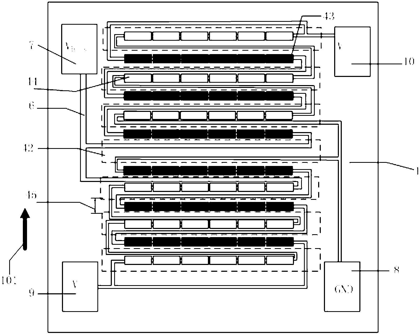
[0089] The difference between this embodiment and the second embodiment is that a Wheatstone quasi-bridge circuit is used. The single-chip bridge magnetic field sensor includes three pads, and the three pads are respectively the first pad for ground bias and the first pad for ground bias. Based on the second pad and the third pad of the output, the Wheatstone quasi-bridge also includes two identical current sources (I1, I2), a reference arm R1 and a sensing arm S1, current sources (I1, I2), Each of the reference arm R1 and the sensing arm S1 has a first end and a second end, and the first pad is connected to the first end of the reference arm R1, the first end of the sensing arm S1 and the second end of the current source (I1, I2). One end is electrically connected, the second pad is electrically connected to the second end of the reference arm R1 and the second end of the current source I2, and the third pad is electrically connected to the second end of the sensing arm S1 and...


PUM


Abstract

The invention relates to a single-chip bridge-type magnetic field sensor which comprises a substrate, reference arms, sensing arms, shielding structures and bonding pads, wherein each reference arm and each sensing arm are respectively provided with at least two rows / lines of reference element strands and sensing element strands, each reference element strand and each sensing element strand are formed by one or multiple identical magneto-resistor sensing elements which are electronically connected, the reference element strands and the sensing element strands are arranged and placed in a staggered mode, each magneto-resistor sensing element is one kind of sensing elements selected from AMR, GMR or TMR, each shielding structure is corresponding arranged on each reference element strand, one sensing element strand is located at the interval position between two shielding structures, and one shielding structure is a long-strip-shaped array which is made of soft magnetic materials permalloy. The single-chip bridge-type magnetic field sensor can be achieved in three bridge structures such as quasi bridge, half bridge and full bridge. The single-chip bridge-type magnetic field sensor has the advantages of being small in size, low in cost, small in offset, high in sensitivity, and good in linearity and temperature stability.

Description

technical field [0001] The invention relates to the technical field of magnetic sensors, in particular to a single-chip bridge-type magnetic field sensor with low offset. Background technique [0002] TMR (Tunnel MagnetoResistance) sensor is a new type of magnetoresistance effect sensor that has been applied in the industrial field in recent years. The sensor uses the tunneling magnetoresistance effect of the magnetic multilayer film material to sense the magnetic field, which is mainly manifested in: in the magnetic multilayer film material, with the change of the magnitude and direction of the external magnetic field, the resistance of the magnetic multilayer film will change significantly. Variety. It has a larger resistance change rate than the previously discovered and practically applied AMR (Anisotropic MagnetoResistance) and GMR (Giant MagnetoResistance, Giant MagnetoResistance) sensors, and has better performance than Hall sensors. temperature stability. [0003]...

Claims


Application Information

Patent Timeline
Patent Type & Authority Applications(China)
IPC IPC(8): G01R33/09
CPCG01R33/09G01R17/105
Inventor 詹姆斯·G·迪克
Owner MULTIDIMENSION TECH CO LTD
Why Eureka
Try Eureka