

Organic sun-blind UV detectors
A technology of solar blindness and ultraviolet light, applied in the field of detectors, can solve the problems of narrowing the selection space of organic materials and increasing the difficulty of device design, and achieves the effect of low price and convenient processing
- Summary
- Abstract
- Description
- Claims
- Application Information
AI Technical Summary
Problems solved by technology
Method used
Image

Examples
Embodiment 1
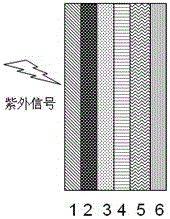
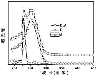
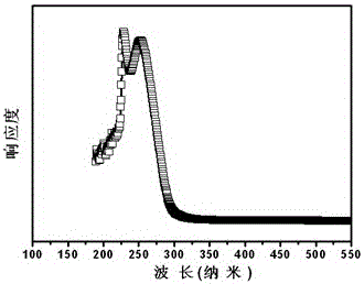
[0032] The glass substrate was ultrasonically washed with detergent, isopropanol, ethanol, and acetone in sequence for 5 minutes, then rinsed with deionized water and dried. A layer of metal aluminum with a thickness of 2 nm was vacuum-deposited on a glass substrate, and after UV-ozone treatment, a PEDOT:PSS (polyaniline derivative) hole transport layer with a thickness of about 40 nm was prepared by spin coating, 120° Bake at C for 15 minutes and take out. D (n=1) was chosen as the donor material, and A (R was pyrazine) as the acceptor material. First, D with a thickness of about 30 nm was prepared on PEDOT:PSS by spin coating, and then A with a thickness of about 20 nm was prepared on the D film by vacuum evaporation. The above two layers constitute the organic activity of the planar heterojunction structure. Floor. Finally, 1 nm thick LiF and 100 nm thick aluminum electrodes were sequentially prepared by vacuum evaporation. As above, get figure 1 The organic solar-blind...
Embodiment 2
[0034] The quartz substrate was ultrasonically washed with detergent, isopropanol, ethanol, and acetone in sequence for 5 minutes, then rinsed with deionized water and dried. A layer of metallic silver with a thickness of 30 nm was vacuum-deposited on a quartz substrate, and after UV-ozone treatment, a PEDOT:PSS (polyaniline derivative) hole transport layer with a thickness of about 40 nm was prepared by spin coating at 120°C Remove after 15 minutes of baking. D (n=2) was chosen as the donor material, and A (R was pyridine) as the acceptor material. A mixed film with a thickness of about 70 nm was prepared on PEDOT:PSS by vacuum mixed evaporation. During the preparation process, by controlling the evaporation rate, the weight ratio of donor:acceptor in the mixed film was 9:1, forming a bulk The organic active layer of the heterojunction structure. Finally, 1 nm thick LiF and 200 nm silver electrodes were prepared sequentially by vacuum evaporation. As above, get figure 1 T...
Embodiment 3
[0036] The quartz substrate was ultrasonically washed with detergent, isopropanol, ethanol, and acetone in sequence for 5 minutes, then rinsed with deionized water and dried. A layer of metal gold with a thickness of 15 nm was vacuum-deposited on a quartz substrate, and after UV-ozone treatment, a PEDOT:PSS (polyaniline derivative) hole transport layer with a thickness of about 40 nm was prepared by spin coating, 120°C Remove after 15 minutes of baking. D (n=3) was chosen as the donor material, and A (R was pyrimidine) as the acceptor material. First, D with a thickness of about 30 nm was prepared on PEDOT:PSS by vacuum evaporation, and then A with a thickness of about 30 nm was prepared on the D film by vacuum evaporation. The above two layers constitute a planar heterojunction structure. active layer. Finally, 1 nm thick LiF and 300 nm gold electrodes were prepared sequentially by vacuum evaporation. As above, get figure 1 Shown is a high-response solar-blind UV light de...
PUM
 Abstract
Description
Claims
Application Information