Diameter transitional czochralski silicon growing method

A Czochralski monocrystalline silicon growth method technology, applied in the direction of single crystal growth, single crystal growth, crystal growth, etc., can solve problems such as waste, increase production time, and reduce production efficiency, so as to reduce production costs and material waste , The effect of simple production process

Active Publication Date: 2013-09-11
ZHEJIANG HAINA SEMICON CO LTD
View PDF12 Cites 14 Cited by
  • Summary
  • Abstract
  • Description
  • Claims
  • Application Information

AI Technical Summary

Problems solved by technology

Due to the limitation of dopant characteristics and single crystal growth process conditions, the axial resistivity of semiconductor single crystal silicon has inhomogeneity. If the customer requires a narrow range of resistivity, there will be some The resistivity is out of gear, and only a small part of single crystals can meet customer requirements, resulting in increased or even wasted inventory of unqualified crystal ingots, and a substantial increa

Method used


Image

  • Diameter transitional czochralski silicon growing method
  • Diameter transitional czochralski silicon growing method
  • Diameter transitional czochralski silicon growing method

Examples


Embodiment 1

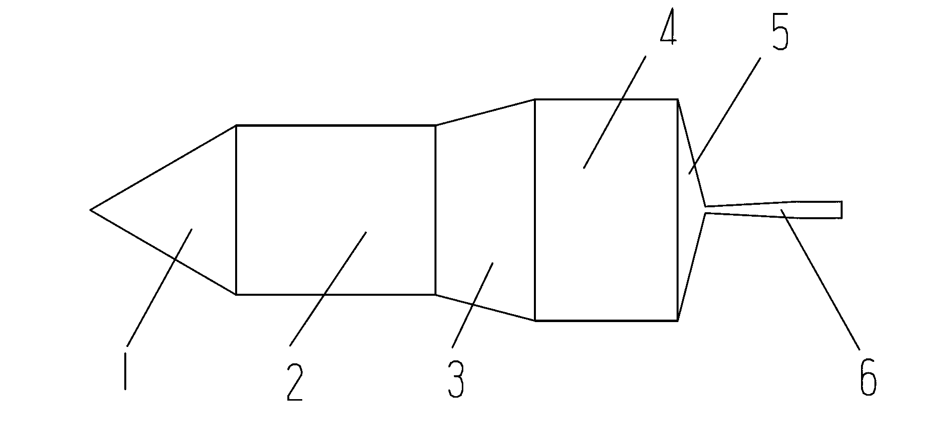
[0027] Embodiment 1, as figure 1 The single crystal silicon rod shown (i.e. No. 1 crystal rod):

[0028] 1. The 8-inch single crystal growth process is adopted, the target resistivity is 58Ω·cm, the pulling speed is 0.5~1.2mm / min, the crystal rotation is 10~20rpm, the crucible rotation is 6~12rpm, and the argon gas flow rate is 30~80slpm. The pressure in the furnace is 12~20torr.

[0029] 2. According to the distribution of the axial resistivity of the 8-inch crystal ingot from the beginning to the end, and the customer's relatively concentrated demand for 8-inch silicon wafers with a resistivity above 55Ω·cm and 6-inch silicon wafers with a resistivity of 45~55Ω·cm, the design Set the equal-diameter length L of an 8-inch single crystal to be 150mm (ie figure 1 The length of the equal-diameter section I4 of No. 1 crystal rod is 150mm).

[0030] 3. When the 8-inch single crystal grows to the target length of 150mm, the resistivity decreases to about 55Ω·cm, and the diameter ...

Embodiment 2

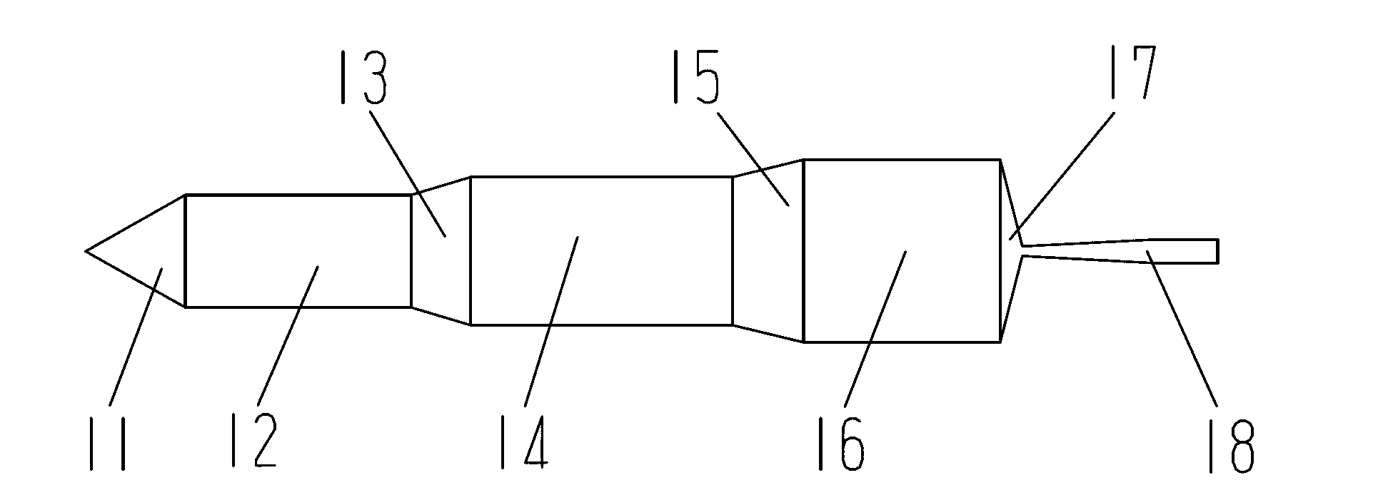
[0034] Embodiment 2, as figure 2 The single crystal silicon rod shown (i.e. No. 2 crystal rod):

[0035] 1. Using a 5-inch single crystal growth process, the target resistivity is 54Ω·cm, the pulling speed is 0.6~1.6mm / min, the crystal rotation is 10~20rpm, the crucible rotation is 6~12rpm, and the argon gas flow rate is 30~80slpm. The pressure in the furnace is 12~20torr.

[0036] 2. According to the distribution of the axial resistivity of the 5-inch ingot from the beginning to the end, and the customer's relatively concentrated demand for 5-inch silicon wafers with a resistivity above 40Ω·cm and 4-inch silicon wafers with a resistivity of 30~40Ω·cm, the design Set the equal-diameter length L of a 5-inch single crystal to be 320mm (ie figure 2 The length of the equal-diameter section I16 of No. 2 crystal rod is 320mm).

[0037] 3. When the equal diameter of the 5-inch single crystal grows to the target length of 320mm, the resistivity drops to about 40Ω·cm at this time,...

Embodiment 3

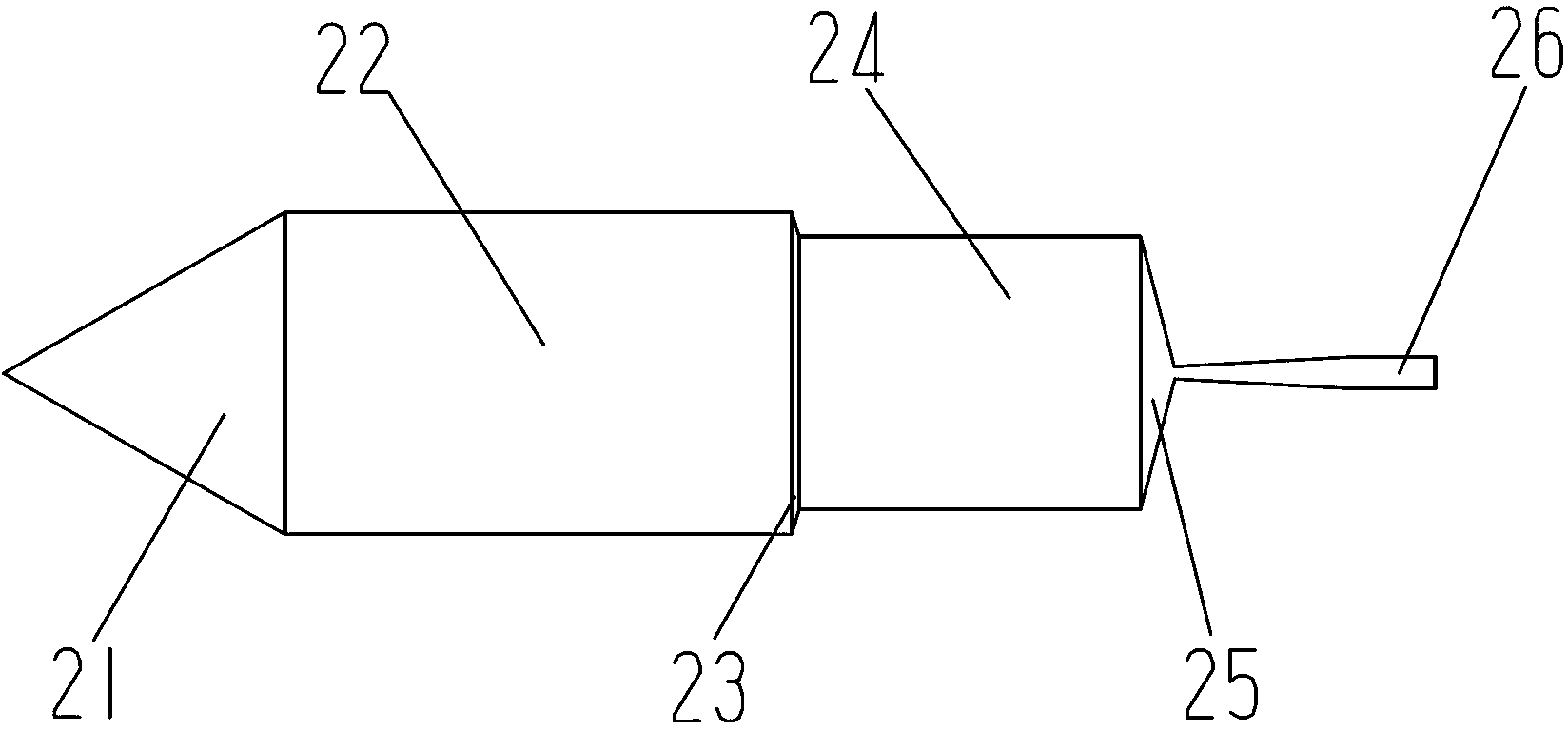
[0045] Embodiment 3, as image 3 The single crystal silicon rod shown (that is, No. 3 crystal rod):

[0046] 1. Using a 5-inch single crystal growth process, the target resistivity is 64Ω cm, the pulling speed is 0.6~1.6mm / min, the crystal rotation is 10~20rpm, the crucible rotation is 6~12rpm, and the argon gas flow rate is 30~80slpm. The pressure in the furnace is 12~20torr.

[0047] 2. Although the market has more demand for 5-inch silicon wafers with a resistivity of 40Ω·cm or more, sometimes customers have more concentrated demand for 5-inch silicon wafers with a resistivity of 55~65Ω·cm. The demand for 55Ω·cm 6-inch silicon wafers is also relatively concentrated. No matter whether it is single-drawing 6-inch single crystal, single-drawing 5-inch single crystal, or pulling 6-inch single crystal first and then turning it into 5-inch single crystal, it cannot be very good. Satisfying the concentrated demand for this grade of resistivity silicon wafers will easily lead to ...


PUM

PropertyMeasurementUnit
Resistivityaaaaaaaaaa

Abstract

The invention discloses a diameter transitional czochralski silicon growing method. The method comprises the following steps of: A, setting a required transitional single crystal diameter and an initial diameter transitional single crystal equal diameter length L according to the axial resistance distribution condition from the head to the tail of a crystal bar; B, carrying out normal czochralski silicon production including steps of melting, temperature stabilizing, guiding the crystal, shouldering, shoulder rotating and the like; C, setting the diameter transitional size and the diameter transitional length according to step A, carrying out a first equal diameter growing step, and when the single crystal equal diameter of the first equal diameter growing step grows to the designated length L, starting the diameter transition; D, after the diameter of the single crystal is turned into the required diameter, carrying out the next equal diameter growing step; and E, completing a closing process after the length of a silicon single crystal bar meets a production requirement.

Description

technical field [0001] The invention relates to the technical field of CZ Czochralski single crystal silicon production, in particular to a diameter-transformed Czochralski single crystal growth method. Background technique [0002] As a semiconductor material, monocrystalline silicon is mainly used in photovoltaic and semiconductor fields. Most semiconductor monocrystalline silicon is manufactured by CZ (Czochralski) Czochralski method. [0003] In the process of manufacturing single crystal silicon by the Czochralski method, silicon crystals grow in a growth chamber, which includes a stainless steel cylinder, an insulation inner cylinder, an insulation outer cylinder, a graphite heater, a quartz crucible, and a graphite crucible. The growth chamber is filled with an inert gas of argon As a protective gas, generally high-purity polysilicon is put into a quartz crucible, heated and melted, and then the molten silicon is slightly cooled to give a certain degree of supercooli...

Claims


Application Information

Patent Timeline
IPC IPC(8): C30B15/22C30B29/06
Inventor 潘金平王伟棱郑欢欣邵晓安应路路郑春松饶伟星王飞尧
Owner ZHEJIANG HAINA SEMICON CO LTD
Why Eureka
Try Eureka