

Copper-platinum alloy wire for connecting in semiconductor apparatus
A platinum alloy and semiconductor technology, which is applied in the field of copper-platinum alloy wire, can solve instability and other problems, and achieve the effect of preventing chip cracking and not improving dynamic strength
- Summary
- Abstract
- Description
- Claims
- Application Information
AI Technical Summary
Problems solved by technology
Method used
Image

Examples
Embodiment Construction
[0054] As Examples 1 to 30 and Comparative Examples 1 to 6, copper alloy thick wires each having a diameter of 5 mm were produced by melting alloys of the compositions shown in Table 1 and performing continuous casting.
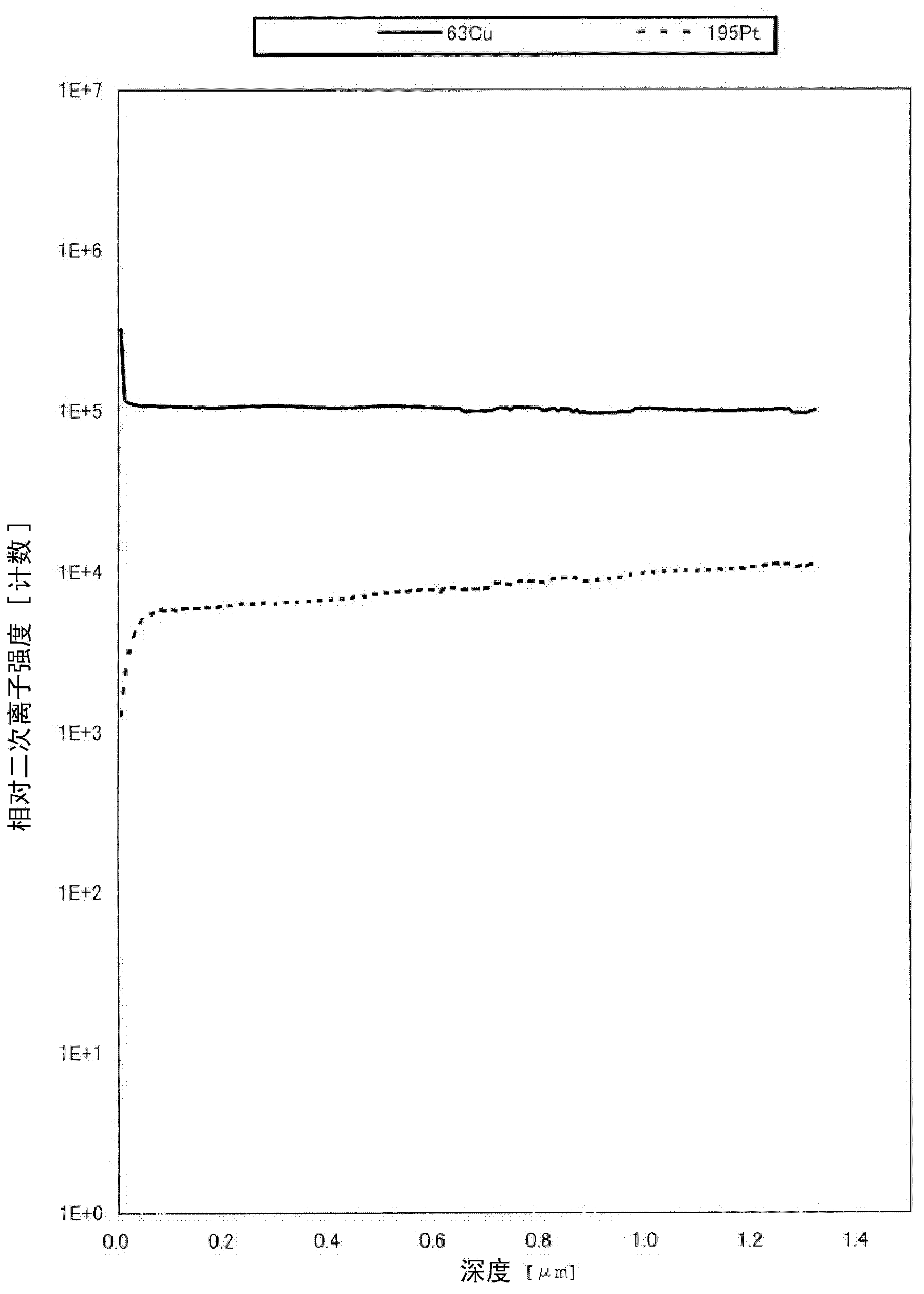
[0055] By the surface of the copper-platinum alloy thick wire of embodiment 1, measure platinum (Pt) and copper (Cu) by SIMS mass spectrometer respectively ( figure 1 ) and the concentration of oxygen (O). The horizontal axis of the graph represents the depth (μm) from the surface of the thick line, and the vertical axis represents the relative secondary ion intensity (log) of the depth.
[0056] according to figure 1 , platinum (Pt) is absent on the surface layer, and up to 50 nm, platinum (Pt) has a lower relative secondary ionic strength than the solid solution matrix. In contrast, it is apparent that copper (Cu) has a significantly higher purity near the surface.
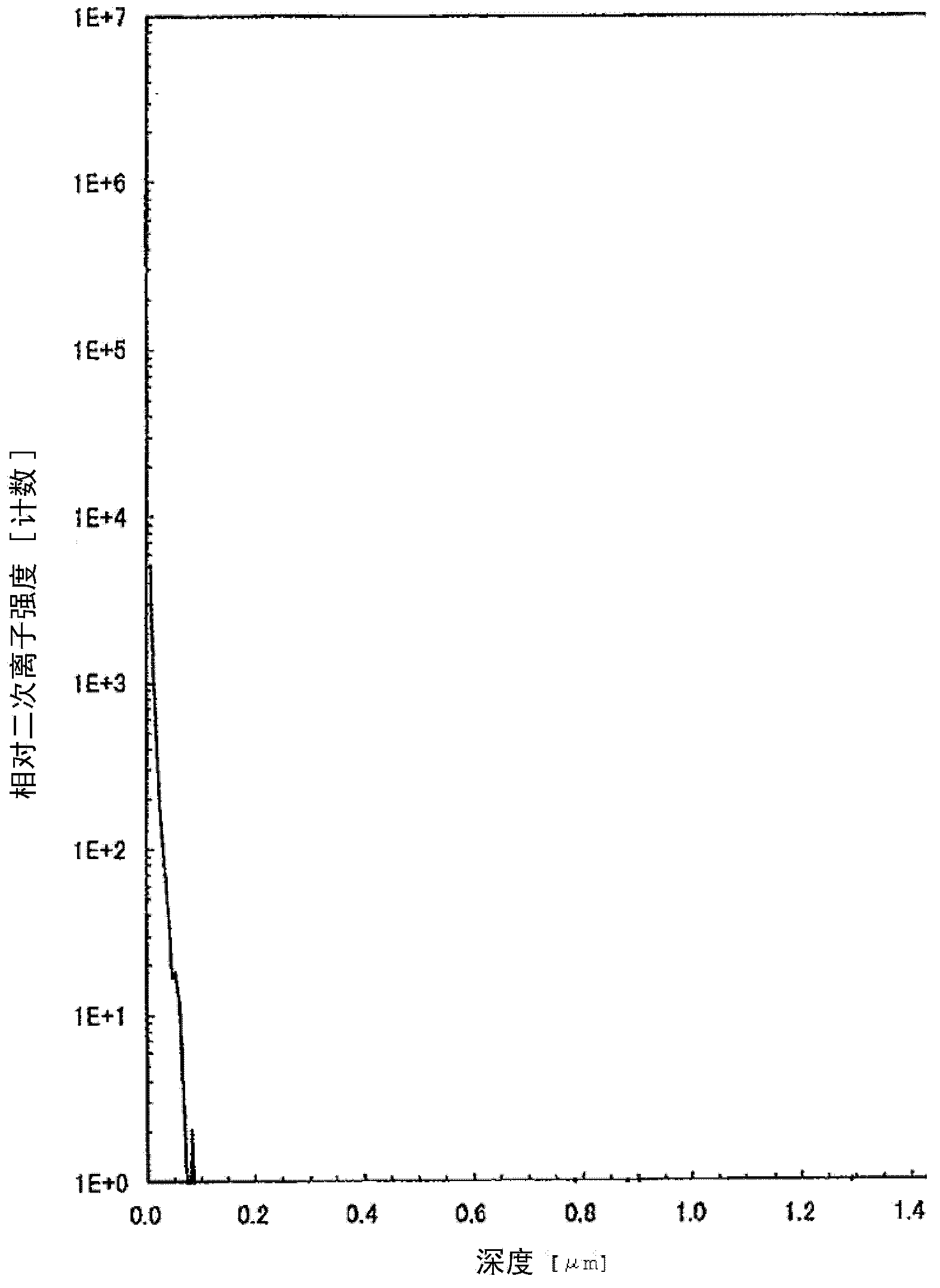
[0057] according to figure 2 , oxygen (O) decreases linearly from the surface layer ...
PUM
| Property | Measurement | Unit |
|---|---|---|
| Diameter | aaaaa | aaaaa |
| Thickness | aaaaa | aaaaa |
| Thickness | aaaaa | aaaaa |
Abstract
Description
Claims
Application Information