A bipolar transistor with improved bvcbo and its production process

A bipolar transistor and production process technology, applied in the electronic field, can solve the problems of reducing the frequency performance of the transistor, the small radius of curvature of the metallurgical junction, and the increase of the transistor area, so as to reduce the parasitic capacitance, high output power, and ensure high frequency performance effect

A bipolar transistor and production process technology, applied in the electronic field, can solve the problems of reducing the frequency performance of the transistor, the small radius of curvature of the metallurgical junction, and the increase of the transistor area, so as to reduce the parasitic capacitance, high output power, and ensure high frequency performance effect

CN103296072BActive Publication Date: 2016-08-10江苏博普电子科技有限责任公司

Image

  • A bipolar transistor with improved bvcbo and its production process
  • A bipolar transistor with improved bvcbo and its production process
  • A bipolar transistor with improved bvcbo and its production process

Examples


Embodiment Construction

[0030] The present invention will be further described below in conjunction with the accompanying drawings of the specification.

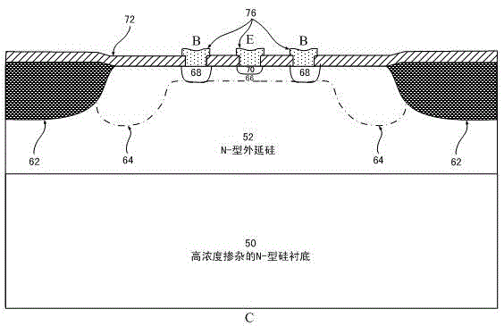
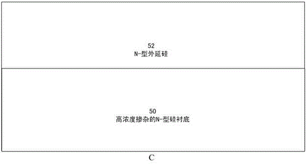
[0031] Such as figure 1 As shown, a bipolar transistor with improved BVcbo. Since the back of the wafer is used to form the collector C of the NPN transistor, in order to reduce the series resistance of the collector, we choose high-concentration doped N-type silicon The substrate 50 serves as the extrinsic collector region of the transistor, the top of the N-type silicon substrate 50 is provided with N-type epitaxial silicon 52 as the intrinsic collector region of the transistor, and both sides of the N-type epitaxial silicon 52 A flat oxide layer 62 is formed by trenching, oxidation, and planarization technology. The upper surface of the N-type epitaxial silicon 52 between the two flat oxide layers 62 is provided with an intrinsic base region 66. Extrinsic base regions 68 are provided on both sides of the region 66, and emitter regions 70 are also p...


PUM


Abstract

The invention discloses a bipolar transistor with improved break voltage of collector-based open emitter (BVcbc) and a production process thereof. The groove field oxidation isolation technology is combined with the junction terminal technology, the groove field oxidation process is divided into two steps, junction terminal boron ion implantation is performed between the two field oxidation steps, and therefore the reasonable junction terminal boron junction depth can be obtained and the technological process is simplified. A junction terminal boron ion implantation window is not needed to be aligned with the groove edge so that the fixed boron doping concentration can be obtained at the junction position of junction terminals and a groove, and the stable BVcbc can be obtained. The BVcbc of NPN silicon bipolar microwave power transistor devices produced through the production process is improved to be above 20V, high output power can be provided, collector junction stray capacitance is reduced, and the device high-frequency performance is ensured.

Description

Technical field [0001] The invention relates to a bipolar transistor with improved BVcbo (collector-base breakdown voltage) and a production process thereof, and belongs to the field of electronic technology. Background technique [0002] High frequency power transistor devices are widely used in communication systems and radar systems. The application design of microwave power transistor devices requires high output power and high gain, and the operating frequency ranges from several hundred MHz to several GHz. In order to achieve such high output power, high gain, and high frequency requirements, in addition to optimizing the layout of the chip device, the selection of process parameters, and the packaging, the improvement of the transistor chip production process is sometimes more important. The reasons are as follows: [0003] 1. In order to obtain high output power, the highest possible doping concentration of the collector should be selected to suppress the saturation of the...

Claims


Application Information

Patent Timeline
10 Aug 2016
Publication
CN103296072B
IPC
H01L29/73; H01L29/06; H01L21/331
Inventors
陈强; 张复才