PCB (printed circuit board) back drilling method

A back-drilling and drilling rig technology, applied in the field of communications, can solve the problems of poor transmission signal integrity, inability to meet the requirements of interlayer alignment, ringing, etc., to reduce the uniformity of plate thickness and eliminate adverse effects.

Active Publication Date: 2013-09-18
GUANGZHOU FASTPRINT CIRCUIT TECH
View PDF7 Cites 33 Cited by
  • Summary
  • Abstract
  • Description
  • Claims
  • Application Information

AI Technical Summary

Problems solved by technology

[0002] With the rapid development of electronic information technology, printed circuit boards (referred to as PCB) are developing in the direction of high density, high integration, high speed and high frequency. There are usually three ways to achieve interlayer interconnection in PCB manufacturing. : 1. Blind hole technology, but due to the limitation of electroplating capacity, the depth-to-diameter ratio of blind holes in the industry is currently 1:1; 2. Multiple pressing technology, for high-thickness-to-diameter ratios to achieve high-density interlayer interconnections (such as HDI board) adopts multiple lamination technology, but when the interlayer interconnection overlaps, there is a problem that the interlayer alignment requirements cannot be met; 3. Back drilling technology, which partially demetallizes the metallized holes, and the removal does not play any role The through-hole section for connection or transmission realizes the interlayer interconnection of PCB parts. Compared with the above two methods, this method has simple process and low production cost, but due to the existence of stubs (referred to as stubs) due to back drilling, it is easy to cause signal generation. Problems such as crosstalk, reflection, ringing, etc., will lead to the deterioration of the integrity of the transmission signal, especially for high-frequency signals. The stub refers to the length of the metal hole wall from the back-drilling fracture layer to the target layer

Method used


Image

  • PCB (printed circuit board) back drilling method
  • PCB (printed circuit board) back drilling method

Examples


Embodiment Construction

[0018] The embodiments of the present invention will be described in detail below in conjunction with the drawings:

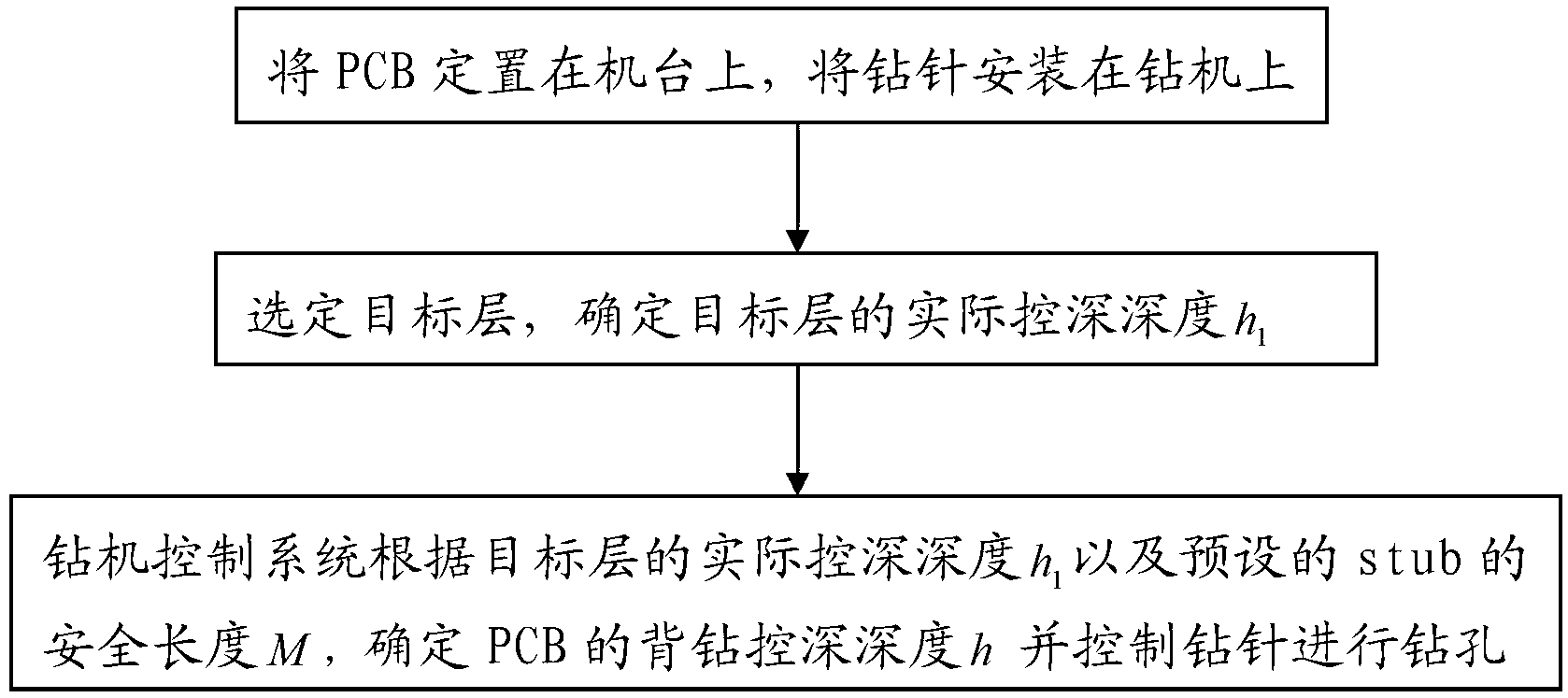
[0019] Such as figure 1 , figure 2 As shown, a PCB back drilling method includes the following steps:

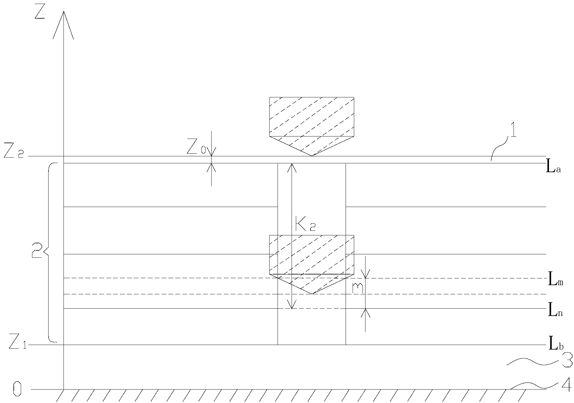
[0020] Set PCB2 on machine 4 and install the drill pin on the drill; make sure machine 4 is the reference plane, the normal line of this plane is upward is the positive direction of Z axis, and the coordinate value of machine Z axis is 0. A conductive cover plate 1 is fixed to the drill face. The conductive cover plate 1 is an aluminum sheet. The conductive cover plate 1 is fixed to the PCB back drill face by masking glue. An aluminum sheet with good conductivity is selected as the conductive cover The conductive cover plate is fixed on the bottom drill surface of the PCB back drill through masking glue to prevent the conductive cover plate from shifting and affect the accuracy of the measurement data;

[0021] Select the target layer and determine the actual co...


PUM


Abstract

The invention relates to a PCB (printed circuit board) back drilling method. The PCB back drilling method comprises the following steps: fixing a PCB on a machine table, and mounting a drill bit on a drilling machine; selecting a target layer, and determining an actual control depth h1 of the target layer; and determining a back drilling control depth h of the PCB according to the actual control depth h1 of the target layer and a preset safety length M of a stub and controlling the drill bit to drill a hole drilling machine control system. According to the PCB back drilling method, influence of thickness uniformity of the board, cone height of a drill tip and copper/ tin-plating process variation on the accuracy of the control depth can be reduced; and through introduction of the safety length M of the stub, the precision of the PCB back drilling control depth h can be effectively controlled, thus achieving precision control of the stub and eliminating adverse effects of the stub on a signal.

Description

Technical field [0001] The present invention relates to the field of communication technology, in particular to a PCB back drilling method. Background technique [0002] With the rapid development of electronic information technology, printed circuit boards (PCBs for short) are developing in the direction of high density, high integration, high speed and high frequency. In PCB manufacturing, there are usually three ways to achieve interconnection between layers. : 1. Blind hole technology, but due to the limitation of electroplating capacity, the current industry’s blind hole depth-to-diameter ratio capability is 1:1; 2. Multiple pressing technology, for high-thickness-to-diameter ratios to achieve high-density interlayer interconnection (such as HDI board) adopts multiple pressing technology, but when the inter-layer interconnection overlaps, there is a problem that the inter-layer alignment requirements cannot be met; 3. Back-drilling technology, partially demetallizes the meta...

Claims


Application Information

Patent Timeline
Patent Type & Authority Applications(China)
IPC IPC(8): B23B35/00
Inventor 陈蓓任小浪曾志军
Owner GUANGZHOU FASTPRINT CIRCUIT TECH
Why Eureka
Try Eureka