Method for manufacturing reverse-blocking semiconductor element
A technology of reverse blocking and manufacturing methods, which is applied in semiconductor/solid-state device manufacturing, semiconductor devices, electrical components, etc., and can solve the problem of low blocking voltage reverse withstand voltage, insufficient activation of the separation layer, residual crystallization, etc. problem, to achieve the effect of reverse withstand voltage
- Summary
- Abstract
- Description
- Claims
- Application Information
AI Technical Summary
Problems solved by technology
Method used
Image
Examples
Embodiment approach 1
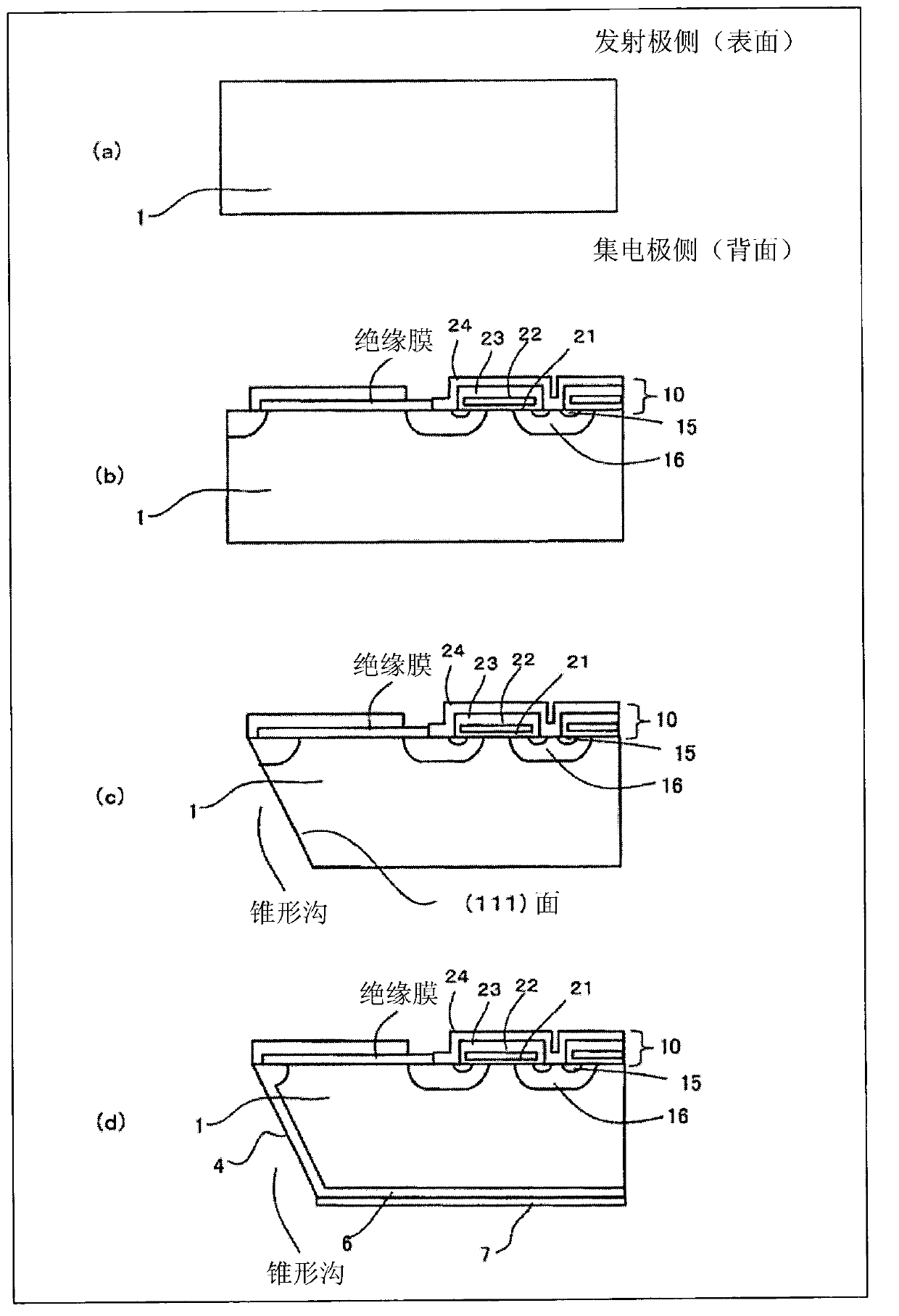
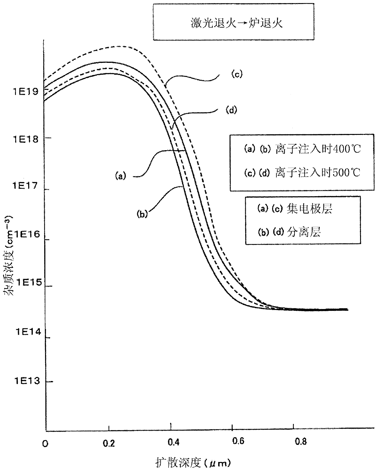
[0129]Embodiments of the reverse blocking type IGBT of the present invention will be described. In order to activate the ion-implanted layers of the collector layer 6 and the separation layer 4 , the ion-implantation is performed while heating the semiconductor substrate 1 during ion-implantation. Further, in order to achieve activation, two annealing treatments, laser annealing treatment and furnace annealing treatment, are performed in this order, which is a characteristic part of the manufacturing method of the reverse blocking semiconductor element of the first embodiment.
[0130] figure 2 It is a graph showing the impurity concentration profiles of the collector layer and the separation layer according to Embodiment 1 of the present invention. exist figure 2 , showing a boron dose of 1 x 10 15 cm -2 , The collector layer ((a), (c)) and the measurement results of the SR concentration distribution on the side surfaces of the separation layer ((b), (d)) (measurement ...
Embodiment approach 2
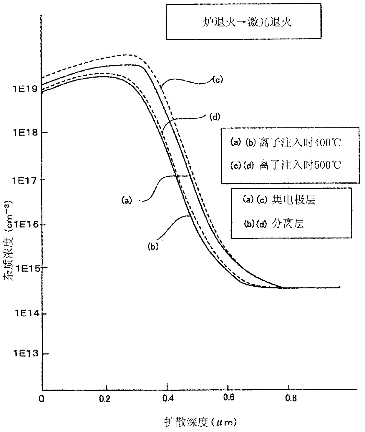
[0134] Next, Embodiment 2 of the reverse blocking type IGBT of the present invention will be described. In order to activate the ion implantation layers of the collector layer 6 and the separation layer 4, the ion implantation is performed while heating the semiconductor substrate 1 to 400° C. to 500° C. during the ion implantation. Then, for further activation, a furnace annealing treatment is first performed, and thereafter a laser annealing treatment is performed.
[0135] image 3 It is an impurity concentration distribution diagram of the collector layer and the separation layer according to Embodiment 2 of the present invention. exist image 3 , showing a boron dose of 1 x 10 15 cm -2 , The collector layer ((a), (c) when the accelerating voltage is 150KeV, and the temperature during ion implantation is 400°C ((a), (b)) and 500°C ((c), (d)) )) and the measurement results of the SR concentration distribution on the side surfaces of the separation layer ((b), (d)) (mea...
PUM
| Property | Measurement | Unit |
|---|---|---|
| thickness | aaaaa | aaaaa |
| thickness | aaaaa | aaaaa |
Abstract
Description
Claims
Application Information
 - R&D Engineer
- R&D Manager
- IP Professional
- Industry Leading Data Capabilities
- Powerful AI technology
- Patent DNA Extraction
Browse by: Latest US Patents, China's latest patents, Technical Efficacy Thesaurus, Application Domain, Technology Topic, Popular Technical Reports.
© 2024 PatSnap. All rights reserved.Legal|Privacy policy|Modern Slavery Act Transparency Statement|Sitemap|About US| Contact US: help@patsnap.com


