Epitaxial wafer of semiconductor light emitting diode and manufacturing method of epitaxial wafer
A technology for light-emitting diodes and epitaxial wafers, applied in semiconductor devices, electrical components, circuits, etc., can solve the problems of poor crystal quality, low luminous efficiency, and poor surface characteristics of the barrier layer in the second multiple quantum well layer, and achieve surface characteristics. Good, high luminous efficiency, good crystal quality effect
- Summary
- Abstract
- Description
- Claims
- Application Information
AI Technical Summary
Problems solved by technology
Method used
Image

Examples
Embodiment 1
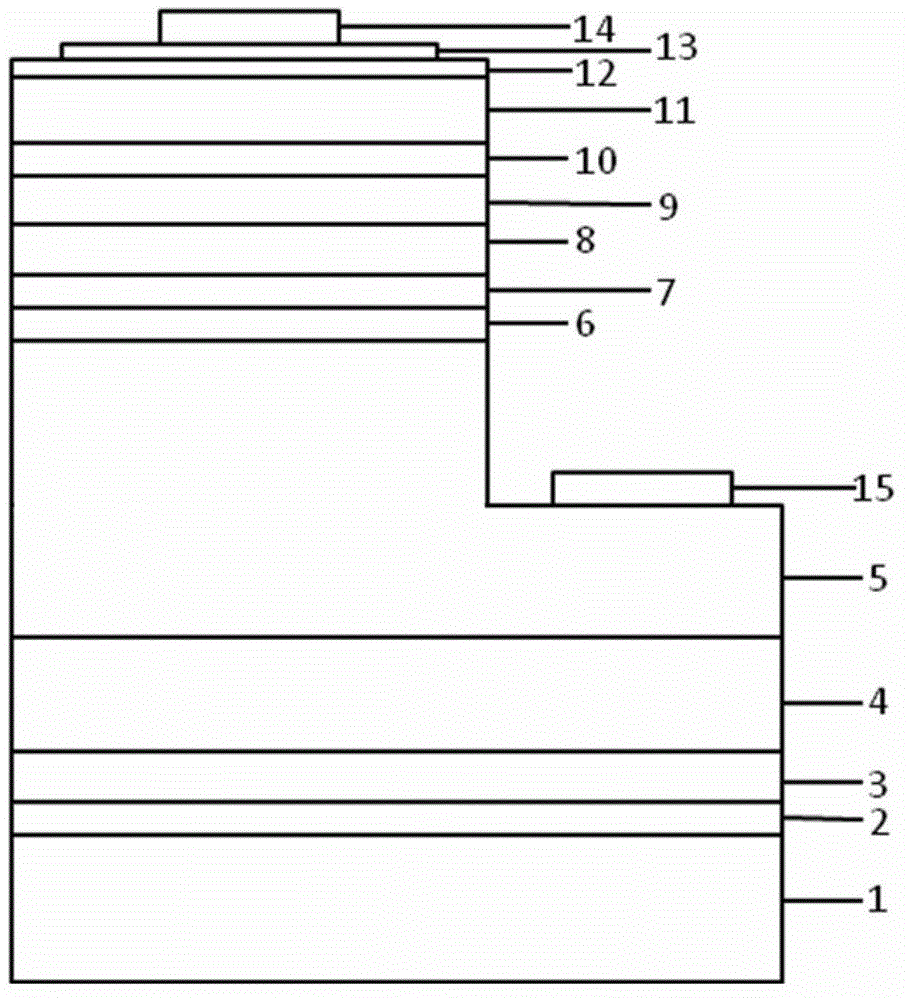
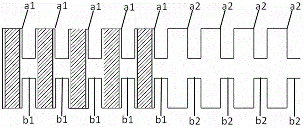
[0028] This embodiment provides an epitaxial wafer of a semiconductor light-emitting diode, participating in figure 1 The epitaxial wafer includes a substrate 1 and a low-temperature buffer layer 2, a high-temperature buffer layer 3, a composite N-type layer, a composite multiple quantum well layer, and a composite P-type layer stacked on the substrate 1 in sequence. The composite multiple quantum well layer includes a first multiple quantum well layer 8 and a second multiple quantum well layer 9 grown on the first multiple quantum well layer 8 . combine figure 2 , the first multi-quantum well layer 8 is a multi-period structure, and each period includes a potential well layer b1 and a barrier layer a1 grown on the potential well layer b1. The barrier layers a1 of each period of the first multi-quantum well layer 8 are respectively doped with Si, figure 2 The hatched area indicates the portion doped with Si in the barrier layer a1.
[0029] Further, in the first multi-qua...
Embodiment 2
[0037] This embodiment provides a method for manufacturing semiconductor light-emitting diode epitaxial wafers, which is implemented by Thomas Swan (AIXTRON subsidiary) CCS MOCVD system, and the method uses high-purity hydrogen (H 2 ) or nitrogen (N 2 ) as carrier gas, trimethylgallium (TMGa) or triethylgallium (TEGa), trimethylaluminum (TMAl), trimethylindium (TMIn) and ammonia (NH 3 ) as Ga, Al, In and N sources respectively, with silane (SiH 4 ), and dimagnesium (Cp2Mg) were used as N and P-type dopants, respectively.
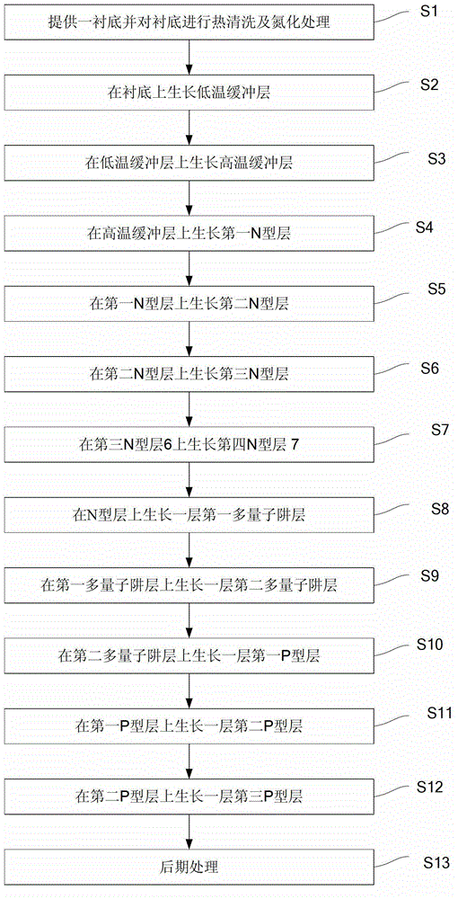
[0038] Specifically, refer to image 3 , and combined with figure 1 and figure 2 In this embodiment, the method for manufacturing a semiconductor light emitting diode epitaxial wafer includes the following steps:
[0039] Step S1, provide a substrate 1 and perform thermal cleaning and nitriding treatment on the substrate 1: thermally clean the surface of the substrate 1 in the temperature range of 1050-1200°C (for example, 1180°C) in a pure hydrogen at...
PUM
 Abstract
Description
Claims
Application Information