Electrotinning method for printed circuit board

A printed circuit board and electro-tinning technology, which is applied in the field of circuit board manufacturing, can solve problems such as insufficient wettability of liquid medicine, affecting quality, and poor tin plating, so as to enhance the exchange capacity of liquid medicine, improve the anti-corrosion performance of tin plating, and avoid unnecessary Effect of Copper Defects

Inactive Publication Date: 2013-10-09
KALEX MULTI LAYER CIRCUIT BOARD (ZHONGSHAN) CO LTD
View PDF0 Cites 8 Cited by
  • Summary
  • Abstract
  • Description
  • Claims
  • Application Information

AI Technical Summary

Problems solved by technology

In the case of over-drawing, often due to the presence of air in the PCB hole, the wettability of the liquid medicine is not enough, resulting in poor tin plating, no copper in the hole and other poor plating defects, exceeding IPC acceptance standards or customer standards, seriously affecting quality problems

Method used


Image

  • Electrotinning method for printed circuit board
  • Electrotinning method for printed circuit board
  • Electrotinning method for printed circuit board

Examples


Embodiment 1

[0043] A kind of electrotinning method of printed circuit board, it comprises the following steps:

[0044] (1) Pre-tinning process:

[0045] (A) Upper plate: place the workpiece on the platen;

[0046](B) Degreasing: Use degreasing agent to degrease the workpiece to make the surface of PCB clean. The concentration of degreasing agent is 100ml / l and the temperature is 40°C;

[0047] (C) Water washing: completely remove the degreasing agent on the surface of the workpiece treated in step (B);

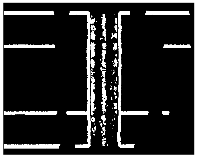
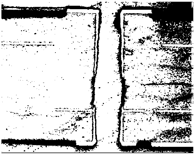
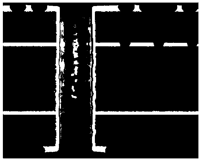
[0048] (D) Micro-etching: Use micro-etching solution to slightly corrode the surface of the workpiece treated in step (C), remove the oxide on the PCB surface and roughen the surface at the same time. The main components of each liter of micro-etching solution include: Na 2 S 2 o 8 Content 50g, 98wt%H 2 SO 4 Content 20ml, Cu 2+ Content 9g (derived from CuSO 4 ·5H 2 O), the temperature is 30°C, and the microetching rate is controlled at 25mg / cm 2 ;

[0049] (E) Washing: complet...

Embodiment 2

[0083] A kind of electrotinning method of printed circuit board, it comprises the following steps:

[0084] (1) Pre-tinning process:

[0085] (A) Upper plate: place the workpiece on the platen;

[0086] (B) Degreasing: Use a degreasing agent to degrease the workpiece to make the surface of the PCB clean. The concentration of the degreasing agent is 80ml / l, and the temperature is 35°C;

[0087] (C) Water washing: completely remove the degreasing agent on the surface of the workpiece treated in step (B);

[0088] (D) Micro-etching: Use micro-etching solution to slightly corrode the surface of the workpiece treated in step (C), remove the oxide on the PCB surface and roughen the surface at the same time. The main components of each liter of micro-etching solution include: Na 2 S 2 o 8 Content 40g, 98wt%H 2 SO 4 Content is 10ml, Cu 2+ Content 3g (derived from CuSO 4 ·5H 2 O), the temperature is 28°C, and the microetching rate is controlled at 15mg / cm 2 ;

[0089] (E) W...

Embodiment 3

[0103] A kind of electrotinning method of printed circuit board, it comprises the following steps:

[0104] (1) Pre-tinning process:

[0105] (A) Upper plate: place the workpiece on the platen;

[0106] (B) Degreasing: Use degreasing agent to degrease the workpiece to make the surface of PCB clean. The concentration of degreasing agent is 120ml / l and the temperature is 45°C;

[0107] (C) Water washing: completely remove the degreasing agent on the surface of the workpiece treated in step (B);

[0108] (D) Micro-etching: Use micro-etching solution to slightly corrode the surface of the workpiece treated in step (C), remove the oxide on the PCB surface and roughen the surface at the same time. The main components of each liter of micro-etching solution include: Na 2 S 2 o 8 Content 60g, 98wt%H 2 SO 4 Content is 30ml, Cu 2+ Content 15g (derived from CuSO 4 ·5H 2 O), the temperature is 32°C, and the microetching rate is controlled at 35mg / cm 2 ;

[0109] (E) Washing: co...


PUM


Abstract

The invention discloses an electrotinning method for a printed circuit board. The electrotinning method comprises the following steps of: (1) tinning pre-processing process; (2) tinning process and (3) tinning post-processing process, wherein the tinning process in the step (2) comprises the following steps of: (J) primary tinning: carrying out tinning on a workpiece in a tinning cylinder by utilizing tinning liquid, so as to obtain a second workpiece, wherein the soaking time of the workpiece in the tinning liquid is 1-3 seconds; and (K) secondary tinning: carrying out the secondary tinning on the second workpiece in the tinning cylinder by utilizing the tinning liquid. According to the electrotinning method disclosed by the invention, the tinning process comprises two tinning steps; by utilizing the tinning method, when the costs of the time and raw materials are scarcely increased, the liquid medicine wettability is increased, the bubbles are reduced, the tinning is uniform in holes, a copper-free state in tinning bubble holes is avoided, and the quality requirements of electroplating can be well met.

Description

technical field [0001] The invention relates to the field of circuit board manufacturing, in particular to an electro-tinning method for printed circuit boards. Background technique [0002] With the rapid development of electronic technology, whether it is military supplies or circuit boards for communication, circuit boards are developing towards miniaturization and integration. However, circuit boards are increasingly required to have smaller apertures and higher layers and board thicknesses, resulting in an increasingly urgent need for high-aspect-ratio processes. The industry's tests and measures on PCB deep-hole copper plating are relatively mature, but there are not many studies on the anti-corrosion performance of tin plating. In the process of PCB deep-hole processing, the anti-corrosion performance of tin plating is facing a severe test. How to effectively improve the corrosion resistance of the coating, reduce the proportion of copper-free scrap in the hole, and ...

Claims


Application Information

Patent Timeline
Patent Type & Authority Applications(China)
IPC IPC(8): C25D5/10C25D3/30H05K3/42
Inventor 梁炳源崔京京
Owner KALEX MULTI LAYER CIRCUIT BOARD (ZHONGSHAN) CO LTD
Why Eureka
Try Eureka