Method for confirming photoetching technique window through accurate and quantitative defect detection

A technology of defect detection and lithography process, which is applied in the field of integrated circuit manufacturing, can solve problems such as poor accuracy, low data readability, unfavorable lithography process lithography process window confirmation, etc.

Active Publication Date: 2013-10-09
SHANGHAI HUALI MICROELECTRONICS CORP
View PDF3 Cites 14 Cited by
  • Summary
  • Abstract
  • Description
  • Claims
  • Application Information

AI Technical Summary

Problems solved by technology

[0010] In view of the above existing problems, the present invention discloses a method for accurate and quantitative defect detection and confirmation of the lithography process window, so as to overcome the unfavorable conditions of the lithography process and the optimal conditions of the lithography process due to the introduction of noise and other unfavorable factors in the prior art. Confirmation of the process window, and the problems of low data readability and poor accuracy

Method used


Image

  • Method for confirming photoetching technique window through accurate and quantitative defect detection
  • Method for confirming photoetching technique window through accurate and quantitative defect detection
  • Method for confirming photoetching technique window through accurate and quantitative defect detection

Examples


Embodiment Construction

[0032] The present invention will be further described below in conjunction with the accompanying drawings and specific embodiments, but not as a limitation of the present invention. The surface of the wafer is patterned after photolithography and etching.

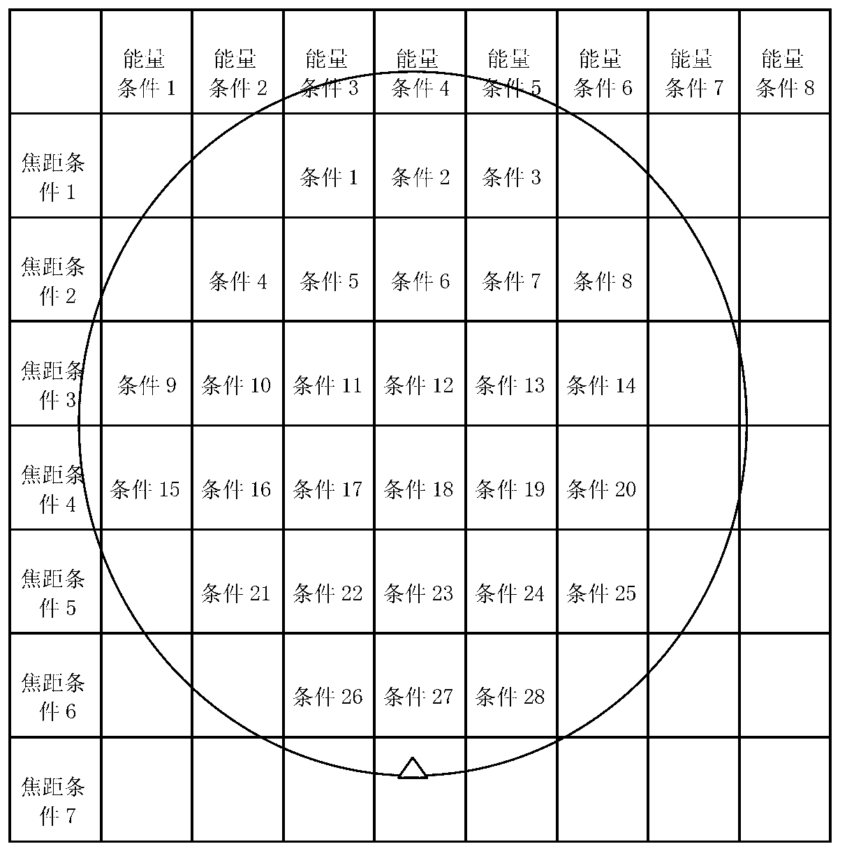
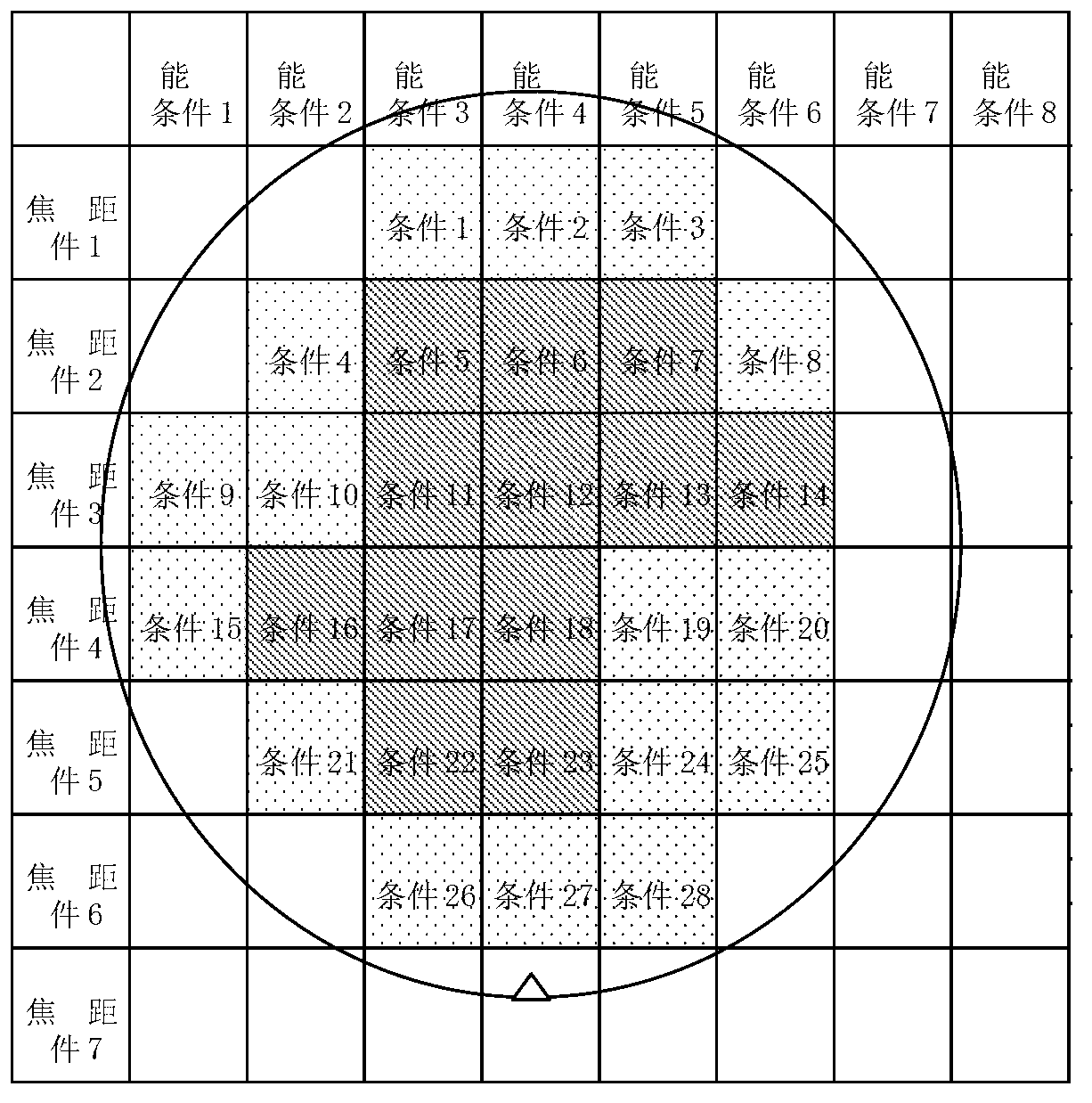
[0033] As an embodiment of the method for accurate and quantitative defect detection and confirmation of the lithography process window of the present invention, it is applied to confirm the lithography process window of the integrated circuit pattern on the wafer, including the following steps:

[0034] Step 1, providing a wafer for confirming the photolithography process window.

[0035]Step 2, setting the reference chip in the wafer, the reference chip is a chip that determines the reference lithography process conditions, that is to say, the set reference chip is a chip that will not have defects, and the reference chip must be selected when setting. For non-defective chips obtained under photolithographic process con...


PUM


Abstract

The invention discloses a method for confirming a photoetching technique window through accurate and quantitative defect detection. The method comprises the following steps: providing a wafer used for confirming the photoetching technique window; setting a benchmark chip in the wafer; distributing and arranging non-benchmark chips in the wafer according to a matrix of photoetching energy and focal length; successively exposing the benchmark chip and the non-benchmark chips; successively performing the defect detection on the exposed benchmark chip and the exposed non-benchmark chips; comparing the defect detection result of the exposed benchmark chip with the defect detection result of the exposed non-benchmark chips to obtain the confirmed photoetching technique window, wherein the benchmark chip is a chip used for determining the benchmark photoetching technique conditions. The method provided by the invention can be used for accurately and quantitatively analyzing a photoetching technique, and obtained photoetching technique window confirmation data have the very good accuracy and the accessible high readability.

Description

technical field [0001] The invention relates to the technical field of integrated circuit manufacturing, in particular to a method for confirming the photolithography process conditions of a wafer photolithography process window, specifically a method for accurate and quantitative defect detection and confirmation of the photolithography process window. Background technique [0002] Counting from the advent of the first transistor, the development of semiconductor technology has been more than half a century, and now it still maintains a strong development trend, continuing to follow Moore's law, that is, the degree of chip integration doubles in 18 months, and the device size every three years Zoom out 0.7 times the speed of development. In the manufacturing process of integrated circuits, multiple processes such as material preparation, masking, photolithography, cleaning, etching, doping, and chemical mechanical polishing have gone through. Among them, the photolithograph...

Claims


Application Information

Patent Timeline
Patent Type & Authority Applications(China)
IPC IPC(8): G03F7/20G06F17/50H01L21/02
Inventor 倪棋梁陈宏璘龙吟
Owner SHANGHAI HUALI MICROELECTRONICS CORP
Why Eureka
Try Eureka