Method for reducing parasitic resistance of graphene top gate FET device

A parasitic resistance and graphene technology is applied in the field of graphene top-gate FET device preparation to achieve the effects of increasing on-state current, improving transconductance and cut-off frequency, and simple process

Inactive Publication Date: 2013-10-09
INST OF MICROELECTRONICS CHINESE ACAD OF SCI
View PDF3 Cites 11 Cited by
  • Summary
  • Abstract
  • Description
  • Claims
  • Application Information

AI Technical Summary

Problems solved by technology

Among them, the channel path resistance between gate-source and gate-drain is determined by the distance between gate-source, gate-drain and graphene surface resistance, while the distance between gate-source and gate-drain is reduced to a certain level due to the limitation of photolithography registration accuracy. Difficult to continue shortening after length

Method used


Image

  • Method for reducing parasitic resistance of graphene top gate FET device
  • Method for reducing parasitic resistance of graphene top gate FET device
  • Method for reducing parasitic resistance of graphene top gate FET device

Examples


Embodiment Construction

[0020] In order to make the object, technical solution and advantages of the present invention clearer, the present invention will be described in further detail below in conjunction with specific embodiments and with reference to the accompanying drawings.

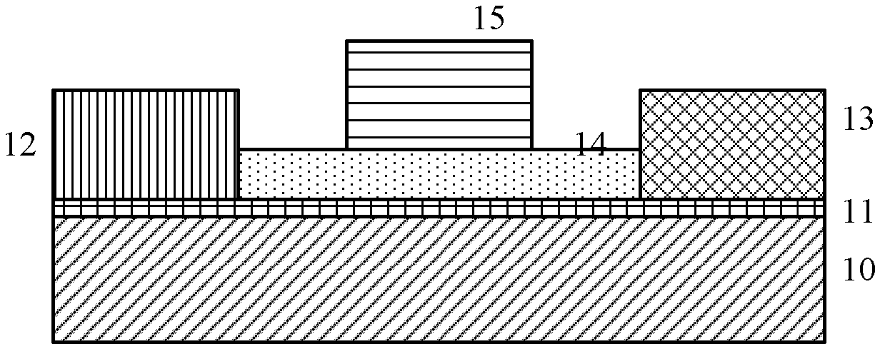
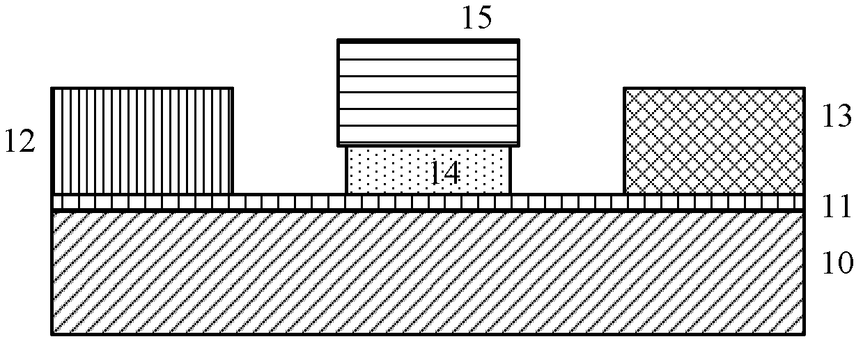
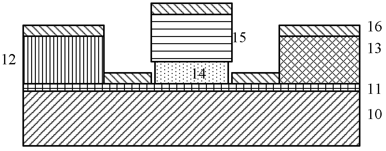
[0021] The invention provides a method for reducing the parasitic resistance of a graphene top-gate FET device. The method is to use the top-gate metal as a mask to protect the top-gate metal lower gate medium, corrode the graphene top-gate FET device, and remove the gate source , the gate dielectric covered on the graphene channel region between the gate and drain, and then vapor-deposit a layer of metal covering the graphene material between the gate source and the gate drain to form a metal graphene contact, eliminating the gap introduced by the distance between the gate source and the gate drain channel resistance. The present invention uses a self-alignment method to vapor-deposit metal to reduce the distance between...


PUM


Abstract

The invention discloses a method for reducing parasitic resistance of a graphene top gate FET device. According to the method, top gate metal is used as a mask for protecting a gate medium below the top gate metal, corrosion is carried out on the graphene top gate FET device to remove the gate medium covering graphene channel regions among a gate source and gate drains, then graphene material among the gate source and the gate drains are covered by a layer of metal in an vapor deposition mode, therefore metal-graphene contact is formed, and channel access resistance introduced by the distance among the gate source and the gate drains is eliminated. An autocollimation technology is adopted for carrying out the vapor deposition on the source drain metal, the access parasitic resistance generated by the distance among the gate source and the gate drains is avoided, so that the ON-state current of the graphene top gate FET device is effectively increased, and transconductance frequency and cut-off frequency of the device are impoved.

Description

technical field [0001] The invention relates to the technical field of preparation of graphene top-gate FET devices, in particular to a method for reducing the parasitic resistance of graphene top-gate FET devices, which uses a self-alignment method to reduce the parasitic resistance of graphene top-gate FET devices , thereby increasing the device signal current, transconductance, gain, and cutoff frequency. Background technique [0002] Nanoelectronics based on graphene is considered to have great application prospects due to the ultra-high carrier mobility and carrier saturation drift velocity of graphene, and it has great potential to replace silicon materials. In the development of graphene top-gate FET devices, parasitic resistance has an important impact on the electrical characteristics of the device, such as on-off current ratio, transconductance, intrinsic gain, and cut-off frequency. Parasitic resistance mainly includes contact metal body resistance, metal graphen...

Claims


Application Information

Patent Timeline
Patent Type & Authority Applications(China)
IPC IPC(8): H01L21/336H01L21/28
Inventor 麻芃金智史敬元张大勇彭松昂陈娇
Owner INST OF MICROELECTRONICS CHINESE ACAD OF SCI
Why Eureka
Try Eureka