TSV wafer reverse side thinning control method and system based on vortex technology

A backside thinning and control method technology, applied in the field of microelectronics, can solve the inability to accurately obtain the distance from the bottom of the conductive metal pillar to the back of the wafer, the influence of etching and other processes, the depth of the hole and the depth of the deposition of the conductive metal pillar error and other problems, to achieve the effect of convenient installation, small measurement error and low process cost

Active Publication Date: 2013-10-09
北京中科微知识产权服务有限公司
View PDF8 Cites 2 Cited by
  • Summary
  • Abstract
  • Description
  • Claims
  • Application Information

AI Technical Summary

Problems solved by technology

[0008] Although the above two methods can calculate the distance from the bottom of the conductive metal pillar to the back of the wafer by measuring the thickness of the entire wafer, in the specific process, the depth of the hole on the wafer and the depth of the deposition of the conductive metal pillar will vary. Therefore, the above method cannot accurately obtain the distance from the bottom of the conductive metal pillar to the back of the wafer, which will have a certain impact on the subsequent etching and other processes.

Method used


Image

  • TSV wafer reverse side thinning control method and system based on vortex technology
  • TSV wafer reverse side thinning control method and system based on vortex technology
  • TSV wafer reverse side thinning control method and system based on vortex technology

Examples


Embodiment Construction

[0032] The present invention will be described in detail below in conjunction with specific embodiments shown in the accompanying drawings. However, these embodiments do not limit the present invention, and any structural, method, or functional changes made by those skilled in the art according to these embodiments are included in the protection scope of the present invention.

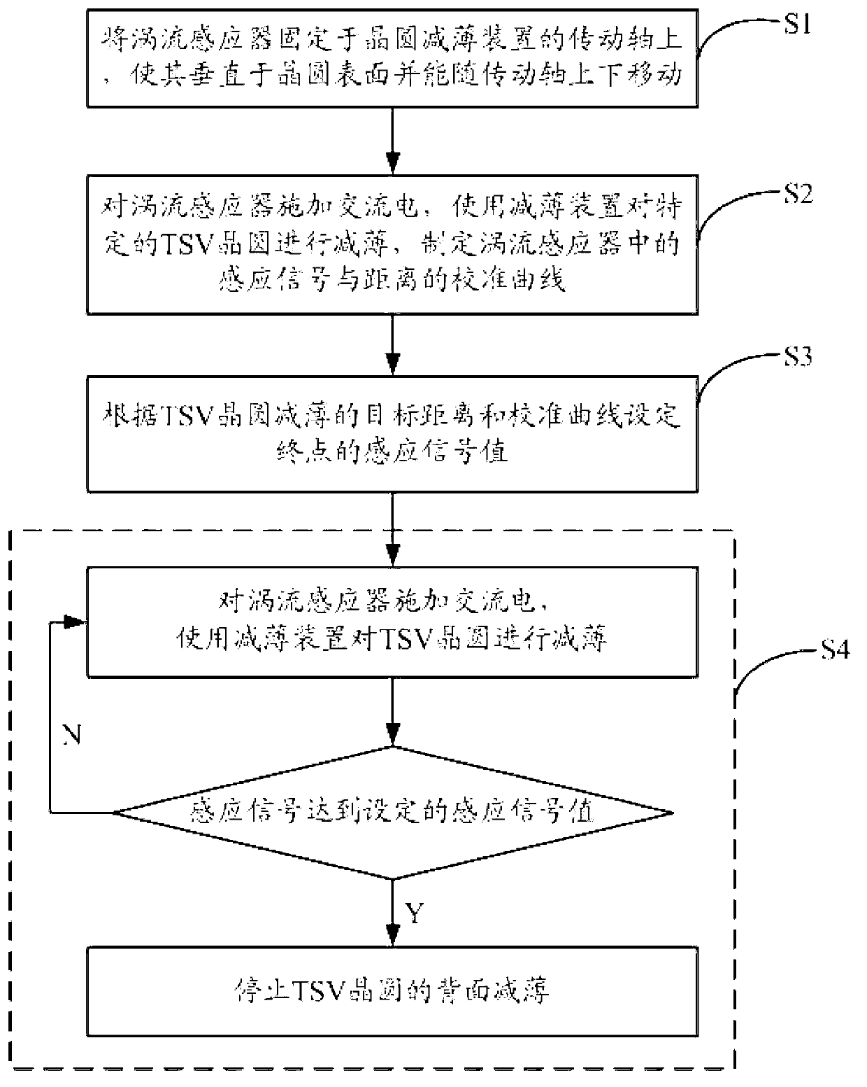
[0033] Such as figure 1 As shown, the TSV wafer backside thinning control method based on eddy current technology in a preferred embodiment of the present invention comprises the following steps:

[0034] S1. Fix the eddy current sensor on the transmission shaft of the wafer thinning device, so that the eddy current sensor is perpendicular to the wafer surface and can move up and down with the transmission shaft;

[0035] S2. Apply alternating current to the eddy current sensor, use a thinning device to thin a specific TSV wafer, and formulate a calibration curve of the induction signal and distance i...


PUM


Abstract

The invention discloses a TSV wafer reverse side thinning control method and system based on the vortex technology. The method includes the steps that a vortex sensor is fixed on a transmission shaft of a wafer thinning device and made to be perpendicular to the surface of a wafer and move up and down along with the transmission shaft; an alternating current is applied to the vortex sensor, the thinning device is used for thinning the specific TSV wafer, and a calibration curve of induction signals and distance of the vertex sensor is formulated; an induction signal value of a terminal point is set according to the thinning target distance of the TSV wafer and the calibration curve; the alternating current is applied to the vortex sensor, the thinning device is used for thinning the TSV wafer, and when the induction signals on the vortex sensor reach the set induction signal value, thinning of the reverse side of the TSV wafer is stopped. The TSV wafer reverse side thinning control method and system effectively achieves non-contact measurement, is small in measuring errors, and can accurately control the thickness of the wafer at the bottom of a metal conductive column. The vortex sensor is convenient to install, and low in process cost.

Description

technical field [0001] The invention relates to the technical field of microelectronics, in particular to a thinning control method and system on the back of a TSV wafer based on eddy current technology. Background technique [0002] With the continuous advancement of microelectronics technology, the feature size of integrated circuits has been continuously reduced, and the interconnection density has been continuously increased. At the same time, users' requirements for high performance and low power consumption have been continuously increased. In this case, the way to improve the performance by further reducing the line width of the interconnection is limited by the physical characteristics of the material and the equipment process, and the resistance-capacitance (RC) delay of the two-dimensional interconnection gradually becomes the limit to improve the performance of the semiconductor chip. bottleneck. [0003] The Through Silicon Via (TSV) process can realize direct t...

Claims


Application Information

Patent Timeline
IPC IPC(8): H01L21/768
Inventor 顾海洋
Owner 北京中科微知识产权服务有限公司
Why Eureka
Try Eureka