Gallium nitride based light emitting diode chip and preparation method thereof

A light-emitting diode, gallium nitride-based technology, applied in electrical components, circuits, semiconductor devices, etc., can solve problems such as the decline of luminous efficiency of LED chips, and achieve the effect of solving the decline of luminous efficiency, reducing the number of cycles, and simplifying process steps

Active Publication Date: 2013-10-09
HEBEI UNIV OF TECH
View PDF11 Cites 14 Cited by
  • Summary
  • Abstract
  • Description
  • Claims
  • Application Information

AI Technical Summary

Problems solved by technology

[0006] The technical problem to be solved by the present invention is to provide a gallium nitride-based light-emitting diode chip and its preparation method, which has a reflected current blocking layer with high impedance and high optical reflectivity in the gallium nitride-based

Method used


Image

  • Gallium nitride based light emitting diode chip and preparation method thereof
  • Gallium nitride based light emitting diode chip and preparation method thereof
  • Gallium nitride based light emitting diode chip and preparation method thereof

Examples


Embodiment

[0050] Step 1, Substrate Formation and Handling

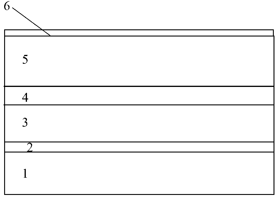
[0051] The epitaxial wafer with LED epitaxial structure grown by MOCVD on a 2-inch sapphire substrate is used as the substrate. The composition of the substrate from bottom to top is: sapphire substrate 1, GaN buffer layer 2, Si-doped n-GaN Layer 3, InGaN / GaN multi-quantum well active region 4 and Mg-doped p-type GaN layer 5, the above substrate was heated at 700°C 2 In a rapid annealing furnace in an ambient atmosphere, a heat treatment process is performed for 60 s to activate the Mg in the Mg-doped p-type GaN layer 5. The substrate obtained by this treatment is soaked in acetone and isopropanol in sequence and then rinsed with deionized water. to remove surface organic contaminants, and then put it into HCl:H 2 Soak in the solution of O=1:5 for 5 minutes, then flush with deionized water for 5 minutes, heat at 80°C in N 2 Dry for 10 minutes until the metal ions attached to the surface are removed;

[0052] The second step ...


PUM

PropertyMeasurementUnit
Thicknessaaaaaaaaaa

Abstract

The invention relates to a gallium nitride based light emitting diode chip and a preparation method thereof, and relates to a semiconductor device provided with at least one electric potential jumping barrier or a surface potential barrier and specially suitable for light emission. The gallium nitride based light emitting diode chip is structurally characterized in that an epitaxial wafer of a conventionally grown LED epitaxy structure in the industry of gallium nitride based light emitting diode chips serves as a substrate, the substrate comprises a sapphire substrate, a GaN buffer layer, a Si doped n type GaN layer, an InGaN / GaN multiple quantum well active area and a Mg doped p type GaN layer from bottom to top, then 1-6 layers of SiO2 / TiO2 distributed Bragg reflection structure layers are alternately deposited, then a composite metal Al film forms a reflected current barrier layer, and an ITO transparent conducting layer in the industry of the gallium nitride based light emitting diode chips is assembled at last. According to the gallium nitride based light emitting diode chip and the preparation method, the current crowding effect on a p metal electrode in the prior art is eliminated, and the problem of LED chip luminous efficiency reduction due to the fact that the metal electrode absorbs photons is resolved.

Description

technical field [0001] The technical solution of the present invention relates to a semiconductor device specially suitable for light emission with at least one potential jump barrier or surface barrier, specifically a gallium nitride-based light-emitting diode chip and its preparation method. Background technique [0002] Gallium nitride-based light-emitting diode chips are the core devices for realizing full-color display panels. The industry demand and technology development trend are large-area chips, high luminous efficiency, high output luminous flux, and cost reduction. [0003] At present, gallium nitride-based light-emitting diode chips are mainly epitaxially obtained on a sapphire substrate by metal-organic compound chemical vapor deposition (hereinafter referred to as MOCVD), and its P-type electrode and N-type electrode are on the same side of the substrate. There is a lateral expansion of the current. Due to the uneven distribution of resistance at the electrode...

Claims


Application Information

Patent Timeline
IPC IPC(8): H01L33/14H01L33/10H01L33/00
Inventor 杨瑞霞张晓洁王静辉田汉民
Owner HEBEI UNIV OF TECH
Why Eureka
Try Eureka