A multilayered composite ceramic layer patterned structure substrate for optical and electronic devices

An electronic device, multi-layer composite technology, applied in the field of electronics, can solve problems such as difficult heat transfer, electrical conduction short circuit, etc., and achieve the effects of solving heat dissipation problems, good electrical isolation and thermal isolation, and effective radial heat conduction and transfer.

Active Publication Date: 2013-10-16
浙江云隐科技有限公司
View PDF5 Cites 21 Cited by
  • Summary
  • Abstract
  • Description
  • Claims
  • Application Information

AI Technical Summary

Problems solved by technology

However, if the multiple optical and / or electronic devices are coupled to a ceramic component with a single interface, it will cause difficulty in heat transfer between the coupled optical and / or electronic devices, and may cause electrical conduction short circuit

Method used


Image

  • A multilayered composite ceramic layer patterned structure substrate for optical and electronic devices
  • A multilayered composite ceramic layer patterned structure substrate for optical and electronic devices

Examples


Embodiment 1

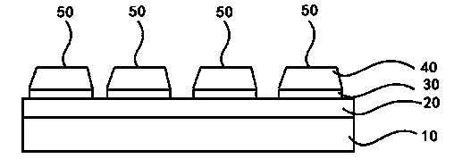
[0022] as attached figure 1 As shown, the multilayer composite ceramic layer patterned structural substrate for optical and electronic devices described in this embodiment includes an aluminum or aluminum alloy substrate 10, on which Al 2 o 3 The pressure-resistant ceramic layer 20 and the AlN high thermal conductivity ceramic layer 40; the Al 2 o 3 There is an active brazing layer 30 between the pressure-resistant ceramic layer 20 and the AlN high thermal conductivity ceramic layer 40, and the high thermal conductivity ceramic layer and the active brazing layer are selectively etched through a mask to form a plurality of isolation bases 50; and A metal circuit layer (not shown in the figure) is formed on the isolation base. The Al 2 o 3 The steps of the pressure-resistant ceramic layer adopt the following process, and the reaction system is AlCl 3 -H 2 O-O 2 -H 2 , the reaction temperature is 420-500°C, the working pressure is 1200Pa, where AlCl 3 The flow rate is 5...

Embodiment 2

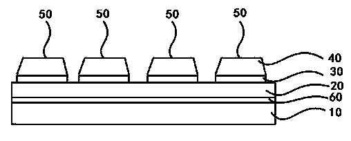
[0024] as attached figure 2 As shown, the multilayer composite ceramic layer patterned structural substrate for optical and electronic devices described in this embodiment includes an aluminum or aluminum alloy substrate 10, on which Al 2 o 3 The pressure-resistant ceramic layer 20 and the AlN high thermal conductivity ceramic layer 40; the Al 2 o 3 There is an active brazing layer 30 between the pressure-resistant ceramic layer 20 and the AlN high thermal conductivity ceramic layer 40; the aluminum or aluminum alloy substrate 10 and the Al 2 o 3 There is an aluminum transition layer 60 between the pressure-resistant ceramic layers 20, and the high thermal conductivity ceramic layer and the active brazing layer are selectively etched through a mask to form a plurality of isolation bases 50; and formed on the isolation bases There are metal circuit layers (not shown in the figure). Wherein, the step of the aluminum transition layer adopts the following process: evacuate t...


PUM


Abstract

The invention relates to a multilayered composite ceramic layer patterned structure substrate for optical and electronic devices. The multilayered composite ceramic layer patterned structure substrate comprises a metal substrate, wherein a voltage-withstanding ceramic layer and a high heat-conducting ceramic layer are sequentially formed on the metal substrate; an active brazing layer is arranged between the voltage-withstanding ceramic layer and the high heat-conducting ceramic layer; multiple isolation bases are formed by selective etching performed on the high heat-conducting ceramic layer and the active brazing layer through a mask; and a metal circuit layer is formed on every isolation base. The multilayered composite ceramic layer patterned structure substrate for optical and electronic devices has a metal substrate in a relatively large size, can accommodate multiple optical and / or electronic devices, and is provided with good electrical isolation and thermal isolation between the multiple optical and / or electronic devices.

Description

technical field [0001] The invention belongs to the field of electronic technology, and more specifically, the invention relates to a multilayer composite ceramic layer patterned structural substrate used for optical and electronic devices. Background technique [0002] Devices used in optics and / or electronics, such as integrated circuits or laser diodes, require the use of thermally conductive materials for heat transfer. For this purpose, a metallic base body is used, for example a copper base body, and an electrical isolation is often required between the optical and / or electronic components and the metal base body. And some ceramic materials have higher heat transfer efficiency and are electrically insulating. For this purpose, highly thermally conductive ceramic materials are frequently used as intermediate materials for providing electrical isolation while still maintaining thermal conductivity between the optical and / or electronic components and the metal base body....

Claims


Application Information

Patent Timeline
Patent Type & Authority Applications(China)
IPC IPC(8): H01L23/15H05K3/02
Inventor 高鞠
Owner 浙江云隐科技有限公司
Why Eureka
Try Eureka