Method for manufacturing surface enhancement Raman scatting substrate

A surface-enhanced Raman and substrate technology, applied in the field of material preparation and Raman spectroscopy, can solve the problems of not being able to achieve high environmental protection, difficult production technology, and high production cost, and achieve easy operation, mature technology, good repeatability, and low cost. low effect

Inactive Publication Date: 2013-10-23
NANKAI UNIV
View PDF5 Cites 16 Cited by
  • Summary
  • Abstract
  • Description
  • Claims
  • Application Information

AI Technical Summary

Problems solved by technology

For example, SERS substrates made by electron beam etching or ion beam etching have properties such as uniformity, repeatability, fine control of structural parameters, and ultra-sensitivity. Large-area SERS substrates of the highest level, the raw materials and technologies used cannot be highly environmentally friendly, so the production technology of this SERS substrate is difficult to be used in practical applications

Method used


Image

  • Method for manufacturing surface enhancement Raman scatting substrate
  • Method for manufacturing surface enhancement Raman scatting substrate
  • Method for manufacturing surface enhancement Raman scatting substrate

Examples


Embodiment Construction

[0029] The following will clearly and completely describe the technical solutions in the embodiments of the present invention with reference to the accompanying drawings in the embodiments of the present invention. Obviously, the described embodiments are only part of the embodiments of the present invention, not all of them. Based on the embodiments of the present invention, all other embodiments obtained by persons of ordinary skill in the art without making creative efforts belong to the protection scope of the present invention.

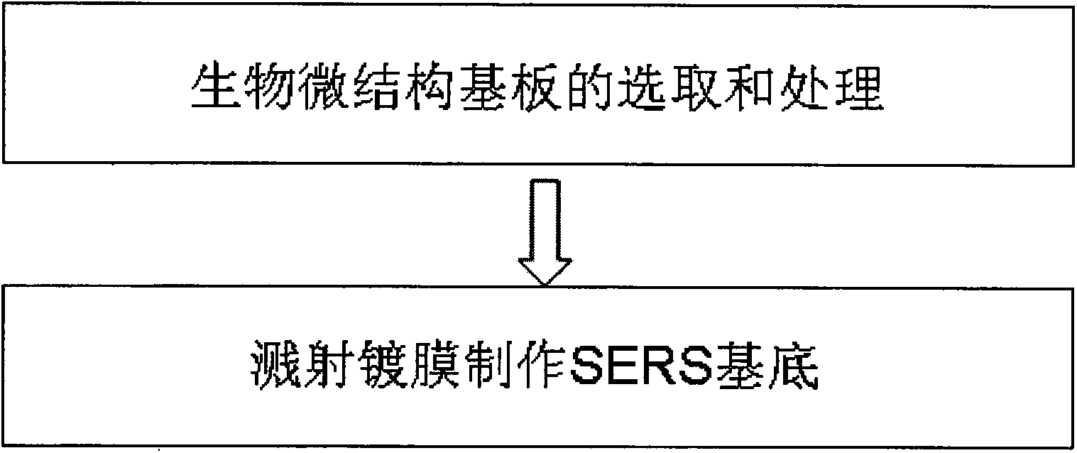
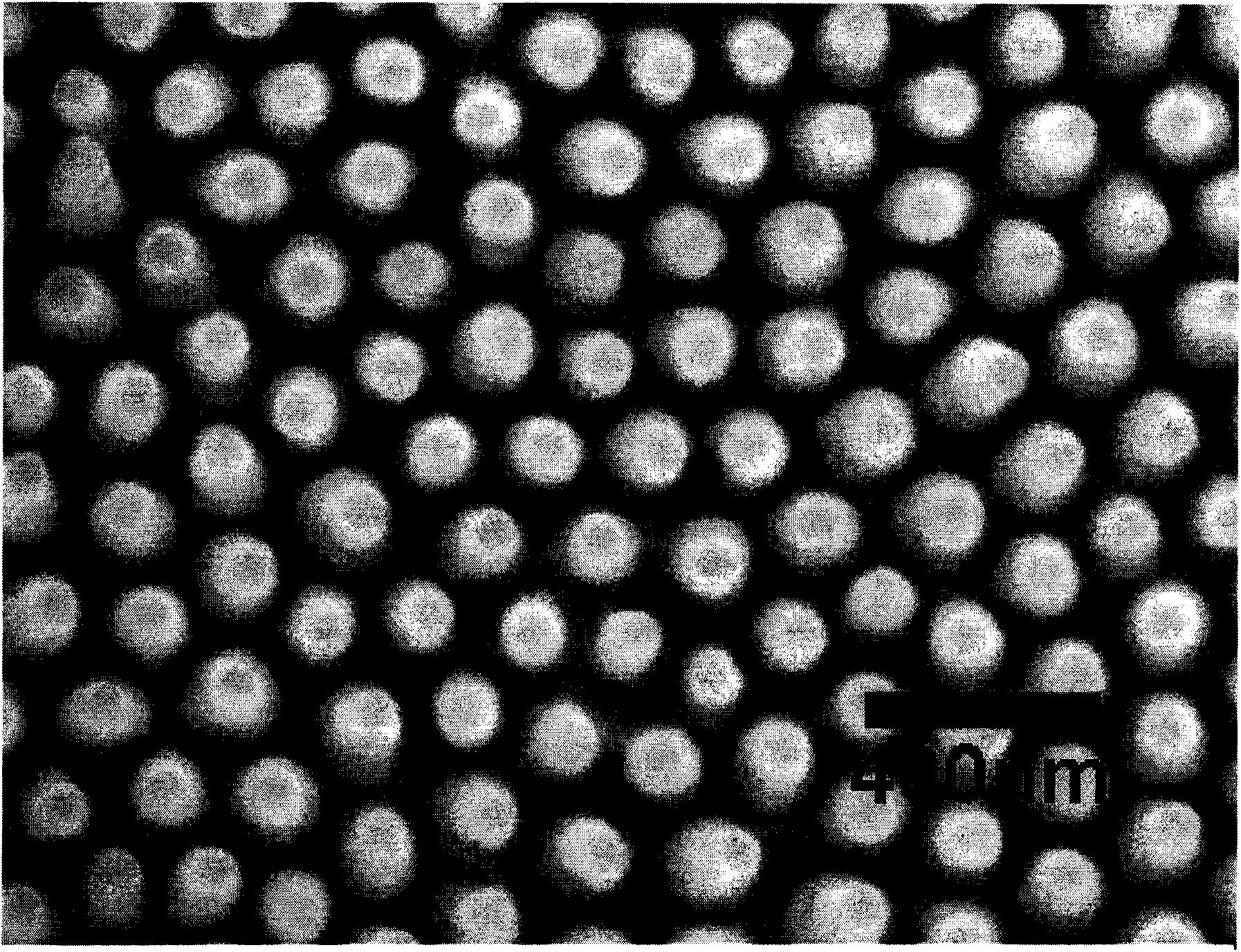
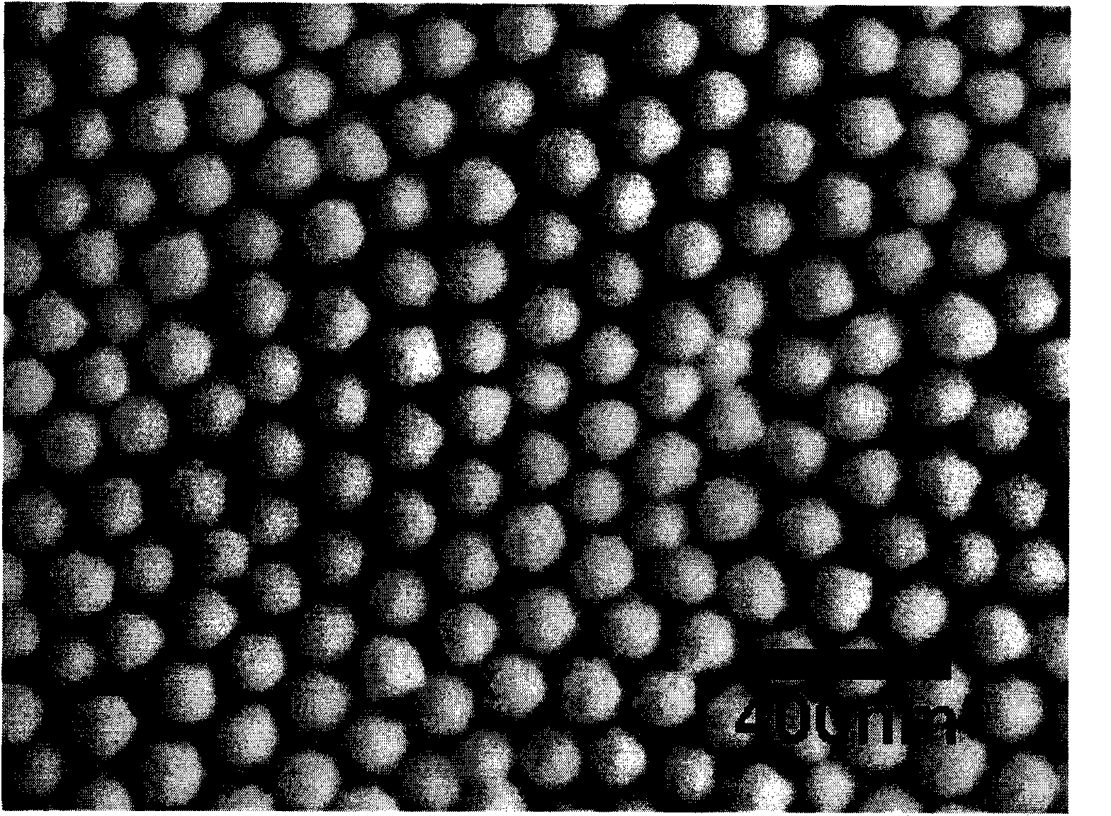
[0030] In order to describe the technical means and efficacy of the present invention in more detail, the preparation method of the SERS substrate proposed in the present invention will be described in more detail below. attached figure 1 Shown is the fabrication process of our SERS substrate.

[0031] (1) Fabrication of biological microstructure substrates. Select an appropriate biological microstructure substrate, wash it, dry it, and reshape...


PUM

PropertyMeasurementUnit
thicknessaaaaaaaaaa
sizeaaaaaaaaaa

Abstract

The invention discloses a method for manufacturing a surface enhancement Raman scatting (SERS) substrate having ultra high performance. The method comprises the steps: firstly, selecting a cicada wing, a butterfly wing, a scarlet macaw feather or other biological micro structures as a basal plate, and simply cleaning, drying and shaping the biological micro structure basal plate; and then plating gold, silver or other precious metals on the biological micro structure basal plate by magnetron sputtering or ion beam sputtering or other precise film plating methods to produce the SERS substrate. The gap size of a micro-nano structure is precisely controlled by controlling the thickness of the plating film, and the micro-nano gap size can be controlled to be less than 10 nm. The manufactured SERS substrate has the outstanding advantages of large area, low cost, uniformity, environmental protection, ultra sensitivity, precisely controllable gap and the like. The environmental protection material is selected as the basal plate, the quite simple, mature and low-cost method is used for manufacturing the high performance SERS substrate which meets the needs of practical applications and theoretical researches, so that a powerful tool and a solid foundation are provided for the theoretical researches and the practical applications of an SERS effect.

Description

technical field [0001] The invention relates to the fields of material preparation, bionics and Raman spectroscopy. It specifically involves using biological micro-nano structures as substrates, depositing gold films by magnetron sputtering or ion beam sputtering technology, and manufacturing large-area, low-cost, uniform, environmentally friendly, and ultra-sensitive surface-enhanced Raman scattering substrates. Background technique [0002] Surface Enhanced Raman Scattering (Surface Enhancement Raman Scatting, SERS) is an ultra-sensitive non-destructive identification and molecular recognition technology. SERS technology has many unique advantages and can provide fast, simple, repeatable, non-destructive qualitative and quantitative analysis. It does not require sample preparation, and samples can be directly measured by fiber optic probes. It is widely used in organic chemistry, polymers, and biology. Surface science, food safety and thin films and many other fields. Th...

Claims


Application Information

Patent Timeline
Patent Type & Authority Applications(China)
IPC IPC(8): C23C14/14C23C14/34G01N21/65
Inventor 齐继伟孙骞吴强李玉栋杨明王午登禹宣伊唐柏权许京军
Owner NANKAI UNIV
Why Eureka
Try Eureka