Method for reducing dead layer of solar cell

A solar cell and dead layer technology, applied in circuits, electrical components, sustainable manufacturing/processing, etc., can solve problems affecting efficiency, poor control of oxide film thickness, etc., achieve the effect of reducing dead layer and improving spectral response

Active Publication Date: 2013-10-23
YINGLI ENERGY CHINA
View PDF7 Cites 12 Cited by
  • Summary
  • Abstract
  • Description
  • Claims
  • Application Information

AI Technical Summary

Problems solved by technology

However, the thickness of the oxide film in the pre-purification step before deposition is not easy to control. If it is too thick, it will affect the formation of the PN junction, thereby affecting the efficiency; if it is to

Method used


Image

  • Method for reducing dead layer of solar cell
  • Method for reducing dead layer of solar cell
  • Method for reducing dead layer of solar cell

Examples


Embodiment Construction

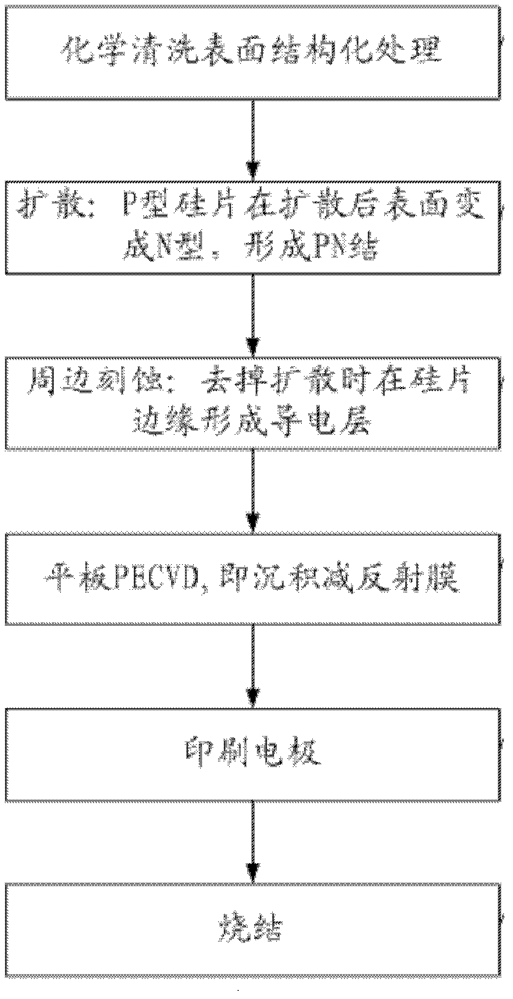
[0027] The invention provides a method for reducing the dead layer of the solar cell to improve the spectral response of the cell.

[0028] The following will clearly and completely describe the technical solutions in the embodiments of the present invention with reference to the accompanying drawings in the embodiments of the present invention. Obviously, the described embodiments are only some, not all, embodiments of the present invention. Based on the embodiments of the present invention, all other embodiments obtained by persons of ordinary skill in the art without making creative efforts belong to the protection scope of the present invention.

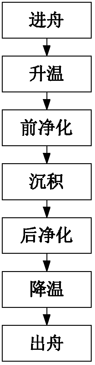
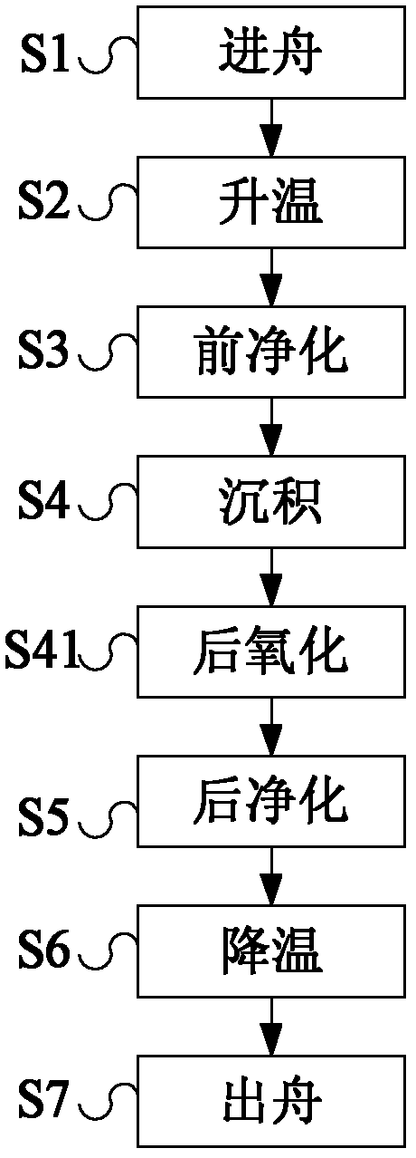
[0029] Please refer to the attached image 3 , image 3 The process flow chart of the method for reducing the dead layer of solar cells provided by the embodiment of the present invention; Figure 4 A process flow chart of a method for reducing the dead layer of a solar cell provided by another embodiment of the present inventi...


PUM


Abstract

The invention provides a method for reducing a dead layer of a solar cell, and the method comprises the steps: 1) boat entering; 2) temperature rise; 3) pre-purification; 4) deposition; 5) post-purification; 6) temperature reduction; 7) boat exiting. The method also comprises: 41) post-oxidation between the step 4) and the step 5) i.e. feeding oxygen for a preset time at a preset temperature by a preset flow or carrying out the post-oxidation step during the step 5). According to the invention, the post-oxidation treatment is added and a certain amount of oxygen is let in after deposition and before the post-purification or in the process of the post-purification. Another layer of oxide film is formed between an oxide film, formed during the pre-purification, and a PN junction. The thickness of the oxide film is increased after the PN junction is formed. Phosphorus atoms react with oxygen after passing through the oxide film and diffusing towards a silicon wafer so as to further reduce the thickness of phosphorus on the surface of the PN junction and decrease the dead layer. Meanwhile, the oxide film is removed after chemical processing to reduce the thickness of the PN junction, so as to effectively improve spectrum response of a cell.

Description

technical field [0001] The invention relates to the technical field of semiconductor processing, and more specifically, relates to a production method of a polycrystalline silicon wafer. Background technique [0002] Crystalline silicon solar cells have been widely used in various fields, and their good stability and mature process flow are the basis for their large-scale application. At present, the manufacturing process of solar cells has been basically standardized, please refer to the attached figure 1 , the main processing flow is as follows: the silicon wafer is cleaned and textured, making the original bright silicon wafer surface uneven, increasing the light absorption rate of the silicon wafer; after high temperature diffusion, the P-type silicon substrate is mixed with N-type impurities, thereby forming a P / N junction; then remove the oxide layer on the side and back of the silicon wafer by plasma etching and dephosphorous silicon glass; deposit a layer of SiNx fi...

Claims


Application Information

Patent Timeline
IPC IPC(8): H01L31/18
CPCY02P70/50
Inventor 王英超李高非崔景光
Owner YINGLI ENERGY CHINA
Why Eureka
Try Eureka