Coating conductor superconducting film and preparation method thereof

A technology of coated conductors and superconducting films, applied in the manufacture/processing of superconductor devices, permanent superconductor devices, etc., can solve the problems of failure to achieve homoepitaxial growth of superconducting layers, failure to achieve overall pinning of superconducting layers, etc. Achieve the effect of increasing thickness, improving purity and improving performance

Active Publication Date: 2013-10-23
NORTHWEST INSTITUTE FOR NON-FERROUS METAL RESEARCH
View PDF6 Cites 6 Cited by
  • Summary
  • Abstract
  • Description
  • Claims
  • Application Information

AI Technical Summary

Problems solved by technology

However, these studies only studied the introduction of defect structures in a specific way, and did not realize the overall pinning of the

Method used


Image

  • Coating conductor superconducting film and preparation method thereof
  • Coating conductor superconducting film and preparation method thereof
  • Coating conductor superconducting film and preparation method thereof

Examples


Embodiment 1

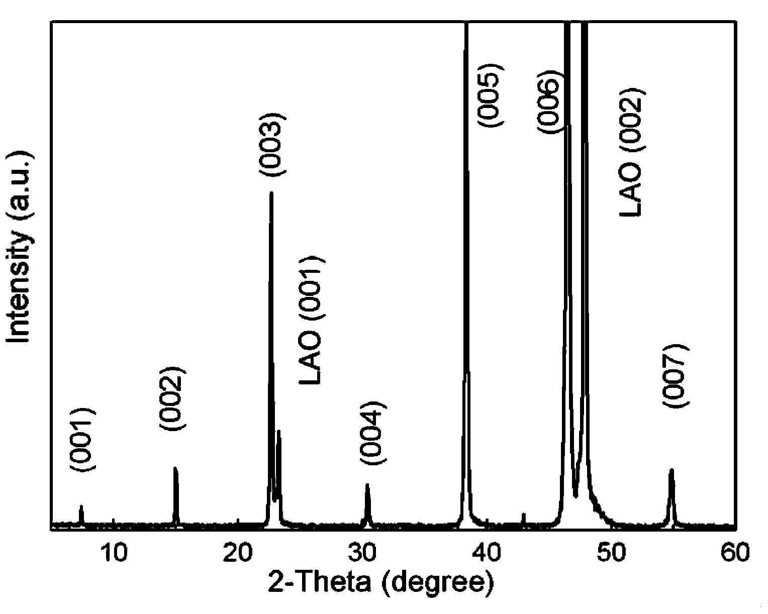
[0030] The superconducting film of this embodiment is made of YHf 0.02 Ba 2.02 Cu 3 o z superconducting layer and covered with YHf 0.02 Ba 2.02 Cu 3 o z Y on the surface of the superconducting layer 0.9 Gd 0.1 Ba 2 Cu 3 o y Film layer composition, where y is 6.8-7, z=y+0.06.

[0031] The preparation method of the coated conductor superconducting film of the present embodiment is:

[0032] Step 1. Combine YBCO powder with BaHfO 3 After the powders are mixed evenly, they are pressed under the condition of 8 MPa for 3 minutes to obtain a compact, and then the compact is sintered at a temperature of 900°C for 8 hours to obtain YBCO and BaHfO 3 The mixed target material, the atomic ratio of Y and Hf in the mixed target material is 1:0.02; then YBCO and BaHfO 3 The mixed target material is deposited on lanthanum aluminate (LAO) single crystal substrate (NiW / CeO can also be used 2 / YSZ / CeO 2 Buffer layer substrate) to obtain YHf with a thickness of 200nm 0.02 Ba 2.0...

Embodiment 2

[0039] The superconducting film of this embodiment is made of YHf 0.04 Ba 2.04 Cu 3 o z superconducting layer and covered with YHf 0.04 Ba 2.04 Cu 3 o z Y on the surface of the superconducting layer 0.9 Gd 0.1 Ba 2 Cu 3 o y Film layer composition, where y is 6.8-7, z=y+0.12.

[0040] The preparation method of the coated conductor superconducting film of the present embodiment is:

[0041] Step 1. Combine YBCO powder with BaHfO 3 After the powders are mixed evenly, they are pressed under the condition of 10MPa for 1min to obtain a compact, and then the compact is sintered at a temperature of 900°C for 10h to obtain YBCO and BaHfO 3 The mixed target material, the atomic ratio of Y and Hf in the mixed target material is 1:0.04; then YBCO and BaHfO 3 The mixed target material is deposited on lanthanum aluminate (LAO) single crystal substrate (NiW / CeO can also be used 2 / YSZ / CeO 2 buffer layer substrate) to obtain a thickness of 300nm YHf 0.04 Ba 2.04 Cu 3 o z S...

Embodiment 3

[0048] The superconducting film of this embodiment is made of YHf 0.035 Ba 2.035 Cu 3 o z superconducting layer and covered with YHf 0.035 Ba 2.035 Cu 3 o z Y on the surface of the superconducting layer 0.9 Gd 0.1 Ba 2 Cu 3 o y Film layer composition, where y is 6.8-7, z=y+0.105.

[0049] The preparation method of the coated conductor superconducting film of the present embodiment is:

[0050] Step 1. Combine YBCO powder with BaHfO 3 After the powders are mixed evenly, they are pressed under the condition of 7 MPa for 5 minutes to obtain a compact, and then the compact is sintered at a temperature of 900°C for 5 hours to obtain YBCO and BaHfO 3 The mixed target material, the atomic ratio of Y and Hf in the mixed target material is 1:0.035; then YBCO and BaHfO 3 Deposition of mixed targets onto NiW / CeO 2 / YSZ / CeO 2 On the buffer layer substrate (lanthanum aluminate single crystal substrate can also be used), a YHf with a thickness of 250nm 0.035 Ba 2.035 Cu 3...


PUM

PropertyMeasurementUnit
Thicknessaaaaaaaaaa
Thicknessaaaaaaaaaa
Thicknessaaaaaaaaaa

Abstract

The invention discloses a coating conductor superconducting film, which consists of a YHfxBa2+xCu3Oz superconducting layer and a Y0.9Gd0.1Ba2Cu3Oy film layer which is coated on the surface of the YHfxBa2+xCu3Oz superconducting layer, wherein x is from 0.02 to 0.04. Moreover, the invention also discloses a preparation method for the superconducting film. The superconducting film disclosed by the invention has defect structures of various types; barium hafnate is introduced into a first layer; ion defects are introduced into a second layer by changing rare earth ion stoichiometric ratio; a second layer film can be induced by nano dot columnar defects of the surface of the first layer to form interface induced pinning centers, and the performance of the superconducting film is improved by the pinning centers formed by the defect structures. According to the superconducting film, a good interface is provided on the basis of the YHfxBa2+xCu3Oz superconducting layer, and thus, the homoepitaxial growth of the second layer film prepared from chemical solution deposition can be promoted to obtain the superconducting film with a biaxial structure. The thickness of the superconducting film is increased.

Description

technical field [0001] The invention belongs to the technical field of thin film materials, and in particular relates to a coated conductor superconducting film and a preparation method thereof. Background technique [0002] The crystal structure of the superconducting layer in the coated conductor has biaxial orientation characteristics, which causes the dependence of the critical current of the superconducting layer on the orientation of the external field. Artificially introducing microscopic defect structures as effective pinning centers is to improve the performance of the coated conductor under a magnetic field. An important path to superconductivity is also a prerequisite for the practical application of coated conductors. There are many types of pinning centers introduced into the superconducting layer, which can be roughly divided into point pinning, line pinning, surface pinning, and bulk pinning according to the morphology and latitude characteristics of the defec...

Claims


Application Information

Patent Timeline
IPC IPC(8): H01L39/14H01L39/24
Inventor 金利华白利锋冯建情李成山王耀卢亚锋于泽铭张平祥
Owner NORTHWEST INSTITUTE FOR NON-FERROUS METAL RESEARCH
Why Eureka
Try Eureka