Graphene-based reflective type saturable absorber and preparation method
A saturable absorption and graphene technology, which is applied in laser components, optics, instruments, etc., can solve the problems of graphene film easy to fall off, enhance light scattering, easy damage, etc., and achieve mass production and high optical damage threshold , the effect of stable performance
- Summary
- Abstract
- Description
- Claims
- Application Information
AI Technical Summary
Problems solved by technology
Method used
Image
Examples
Embodiment 1
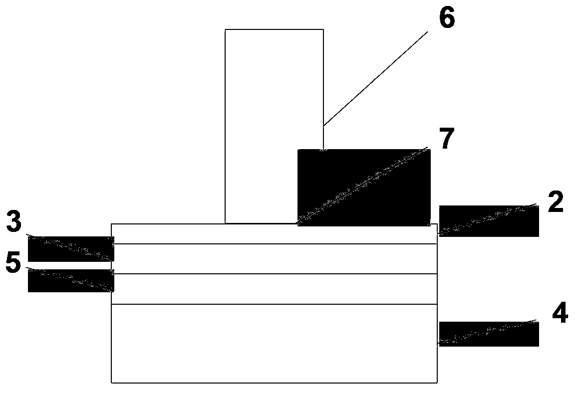
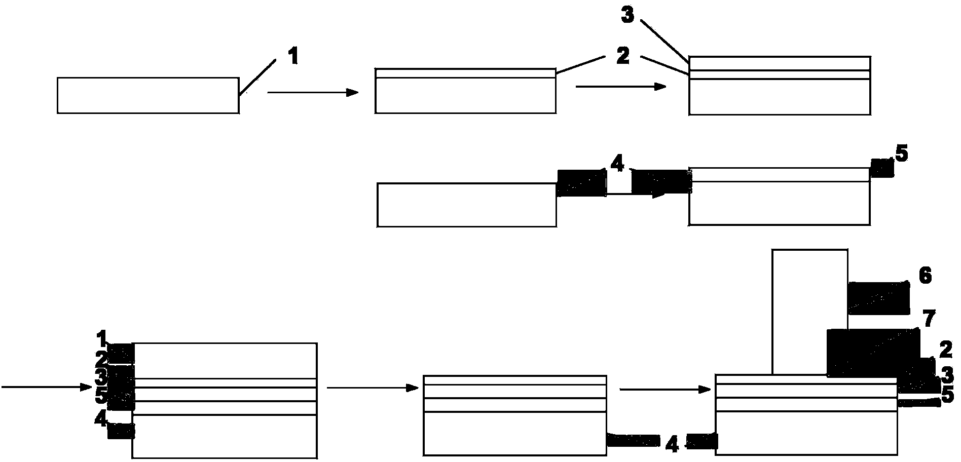
[0040] Combine below figure 2 The graphene-based reflective saturable absorber and its preparation method are introduced in detail. figure 2 Including: copper foil 1, graphene 2, first gold film 3, silicon substrate 4, second gold film 5, optical fiber 6, contact surface 7 between optical fiber and graphene.
[0041] A method for preparing a reflective saturable absorber based on graphene, comprising the following steps:
[0042]Graphene 2 is grown on copper foil 1 by a chemical vapor deposition (CVD) method. First put the copper foil 1 into the quartz tube, raise the temperature to 800-1100°C, then pass in 10-200 sccm of hydrogen for 5-30 minutes, and then pass in one or two gases of methane and acetylene, the gas flow rate is 10 ~300 sccm, after graphene 2 grows for 5~60 minutes, turn off the carbon source gas and cool down rapidly under the hydrogen atmosphere. A first gold film 3 with a thickness of about 200 nm is deposited on the upper surface of the grown graphene ...
Embodiment 2
[0047] Graphene was grown on copper foil by chemical vapor deposition (CVD). First put the copper foil into the quartz tube, the temperature rises to 800-1100°C, then pass in 10-200sccm of hydrogen for 5-30 minutes, and then pass in one or two gases of methane and acetylene, the gas flow rate is 10-200sccm 300 sccm, after 5-60 minutes of graphene growth, turn off the carbon source gas and rapidly cool down in the hydrogen atmosphere. A first silver film with a thickness of about 200 nm is plated on the upper surface of the grown graphene. A second silver film with a thickness similar to that of the first silver film is plated on a silicon dioxide substrate with a thickness of millimeter order. Place the copper foil upwards and place the first silver film downwards. The first silver film and the second silver film are glued together by means of ultraviolet glue, so that the first silver film and the second silver film are integrated, which is the so-called reflection film lay...
PUM
| Property | Measurement | Unit |
|---|---|---|
| thickness | aaaaa | aaaaa |
Abstract
Description
Claims
Application Information
 - R&D
- Intellectual Property
- Life Sciences
- Materials
- Tech Scout
- Unparalleled Data Quality
- Higher Quality Content
- 60% Fewer Hallucinations
Browse by: Latest US Patents, China's latest patents, Technical Efficacy Thesaurus, Application Domain, Technology Topic, Popular Technical Reports.
© 2025 PatSnap. All rights reserved.Legal|Privacy policy|Modern Slavery Act Transparency Statement|Sitemap|About US| Contact US: help@patsnap.com


